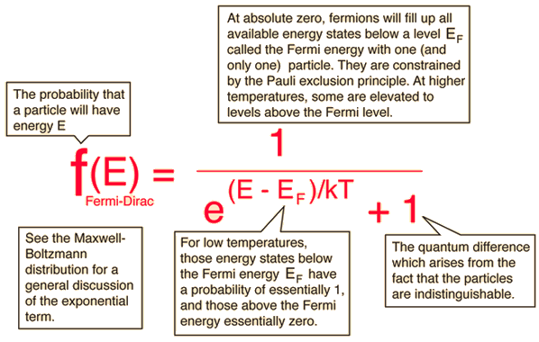
Que.51 What is the significance of the Fermi Dirac function?
Answer:
- The Fermi Dirac function is also known as the Fermi Dirac probability function. It specifies the fraction of all the states at energy E(eV) occupied under thermal equilibrium.
- It does not give the number of electrons in a given energy level.
- It does not give the number of energy levels occupied by electrons.
- Instead, it gives the probability of finding an electron in a given energy state or given energy level.
Que.52 What is the effect of light on intrinsic semiconductors?
Answer: When light falls On the intrinsic Semiconductor because of the photon energy, the surface of the semiconductor gets heated up and due to the heat produced in the semiconductor a large number of covalent bonds will be broken and an equal number of electrons and holes are created. so it increases the conductivity slightly.
Que.53 What are intrinsic and extrinsic excitation?
Answer:
- Intrinsic excitation: when light falls on the intrinsic semiconductor an electron may be excited from the valence band to the conduction band and this is called intrinsic excitation.
- Extrinsic excitation: when light falls on the N-type semiconductor an electron may be excited from the donor energy level into the conduction band or in the case of a P-type semiconductor, an electron may be excited from the valence band to the acceptor energy level.
Que.54 How will you define a Diode?
Answer: A Diode is a non-linear device also known as the unidirectional device as it allows the flow of current in one direction only. It can be used as an active device or passive device depending upon the application.
Que.55 What is a step-graded diode?
Answer:
- Step graded diodes are designed with abrupt junctions i.e. either donor concentration or acceptor concentration will be more. They are not equal.
- The depletion layer will be penetrating more into the lightly doped regions and lesser in the highly doped regions.
- Maximum electric field intensity will be at the junction only.
Que.56 What do you know about solar cells?
Answer:
- The solar cell works on the principle of photovoltaic effect which is the conversion of light energy into voltage..
- It is always operated with forwarding bias.
- Its Characteristics curve is plotted in the 4th quadrant.
- Its cut-in voltage is zero.
- Solar cells are mostly used in satellites, during night time power requirement of the satellite is done by using rechargeable solar batteries.
- Examples of solar cells are CdS solar cells, CdSe, NiCd, ZnS, and PbS.
Que.57 Tell me something about the Schottky diode.
Answer:
It is metal-semiconductor junction diode.
- It is also known as the Schottky barrier or hot cathode diode.
- Current is carried by means of electrons only.
- Switching time is very less.
- It is used across the collector-base junction of the BJT to prevent the BJT from entering saturation.
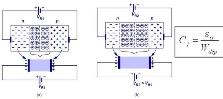
Que.58 What is Diffusion capacitance and transition capacitance?
Answer:
- Diffusion capacitance: In the forward-biased diode, the potential barrier at the junction gets lowered. As a result, holes get injected from the P-side to the N-side and electrons get injected from the N-side to the P-side. These injected charges get stored near the junction just outside the depletion layer, holes in the N-region, and electrons in the P-region. Due to charge storage, the voltage lags behind the current producing the capacitance effect. Such a capacitance is called diffusion capacitance or storage capacitance CD.
- Transition capacitance: With the increase of the magnitude of reverse bias, the majority of carriers move away from the junction i.e. the width W of the depletion layer increases. This uncovered immobile charge on the two sides of the junction constitutes a capacitor of incremental capacitance CT is given by, This capacitance CT is called the transition capacitance or space charge capacitance or barrier capacitance, or depletion layer capacitance.
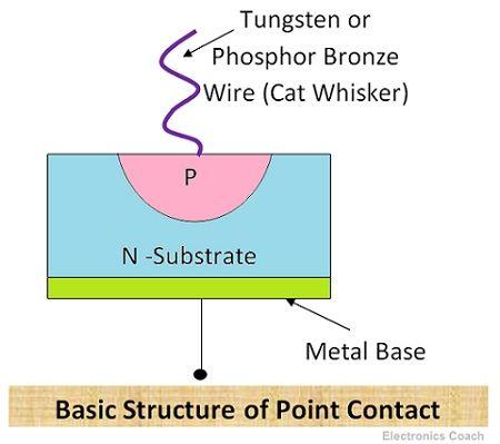
Que.59 Tell me something about the point-contact diode.
Answer:
- It was the first semiconductor diode invented in 1909.
- It is a type of metal-semiconductor junction diode.
- N-type semiconductor diode in which a silver-coated tungsten wire in form of a cat whisker is in contact.
- It is suitable for high-power applications.
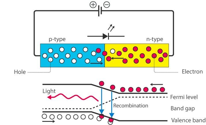
Que.60 On what principles LED work? What are the applications of light-emitting diodes?
Answer:
- LED works on the principle of electro-luminance i.e. conversion of electrical energy into light energy. Light is emitted due to a large number of recombinations at the junction.
- Application of LEDs:
- It is used as a remote control transmitter.
- It is used in designing optocouplers.
- Also used as a display device.
Que.61 Principle of working of LCD and its applications.
Answer: It works on the principle of dynamic scattering of light. Its major application is as a display device.
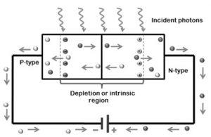
Que.62 On what principle photodiode works? Advantage and disadvantages of the photodiode.
Answer:
- Photodiode works on the principle of photoconductive effect.
- Photoconductive effect- when light falls on the convex lens at the junction, maximum intensity of light will be focused at the junction, so a large number of covalent bonds will be broken and a large number of minority carriers are generated in the device. Which will increase the conductivity of the device.
- Thus basically with an increase in the amount of light, conductivity increase. This is called the photoconductive effect.
- Advantages of photodiode:
- It is 10 times faster than compared to the normal diode.
- It is 100 times more sensitive than a normal diode.
- Disadvantages of photodiode:
- It has a low power handling capacity.
- It is always operated under reverse bias.
Que.63 What are the applications of a photodiode?
Answer: Applications of photodiode are:
- It is used as a remote control sensor.
- It is used in designing optocouplers.
- It is a light-operated switch.
- It is used in photometers.
- It is used in designing the photoconductive sensor.
- It is used to read the audio track recorded on motion picture film.
Que.64 What happens when a forward bias diode is suddenly reverse biased?
Answer: When a forward bias diode is suddenly reversed biased, the diode instantly cannot go to reverse bias. It requires a certain amount of time interval called storage time, meanwhile, majority carriers will be blocked and minority carrier current will flow from n to p until the storage time is over. So diode will continue to remain under forwarding bias. When the time will become greater than storage time, the diode will become reverse biased.
Que.65 What is the tunneling effect? Which diode works on the principle of tunneling effect?
Answer:
- Tunneling effect: occurs in highly doped devices. When doping of 1:10^3 is done on both sides of the p-n junction, because of this doping a very narrow depletion width is formed by degenerate p++ and n++. Due to this narrow width depletion layer formation, there is a chance for electrons to escape through this layer known as the tunneling phenomenon. Charge carriers penetrate the depletion layer with almost the speed of light, as like if there is a tunnel in the device.
- Tunnel diode and Zener diode with abrupt junction are the diodes which work on the principle of the Tunneling effect.
Que.66 What are the applications of Zener diode?
Answer: Applications of Zener diode are:
- It is used in voltage regulator circuits.
- It is used as a switch that is faster than a normal diode.
- It is used as a rectifier.
- It is also used as a clipper or amplitude limiter.
- It is used to convert the given sine waveform to a square wave or a pulse waveform.
Que.67 What are the different breakdown mechanisms on which Zener diode works?
Answer: There are 2 types of breakdown mechanisms on which the Zener diode work:
- Zener breakdown phenomena: is due to large electric field intensity. Occurs at a value less than 6 volts due to tearing or rupturing of covalent bonds in the depletion layer. This is a very sharp breakdown. It occurs in highly doped diodes.
- Avalanche breakdown mechanism: it is due to electron multiplication which occurs due to multiple collisions between electrons and ions in the depletion layer. It is due to impact ionization. It will occur for a voltage greater than 6 volts and it is not very sharp. This effect occurs in the light-doped reverse bias of the Zener diode.
Que.68 What is a tunnel diode? For which application tunnel diode is used?
Answer: It is a highly degenerate PN junction diode with narrow depth depletion layer width that works on the principle of tunneling effect. Charge carriers will be penetrating the narrow depletion layer width with a speed almost at the speed of light as if there is a tunnel in the device.
- Application of tunnel diode:
- It is used in the design of microwave oscillators.
- Used as a voltage-controlled device.
- Used for sawtooth wave generation.
Que.69 Though the tunnel diode is fastest switch, why it is not used as a switch?
Answer: A tunnel diode is never used as a switch because its switching time is very fast. In 1 clock cycle, it goes 1000 times on-off, so its timing diagram cannot be plotted. A truth table cannot be made, hence its logic gate cannot be designed.
Que.70 Diodes which work as negative resistance devices?
Answer: Most important negative resistance devices are:
- tunnel diode: it exhibits negative resistance property when the device changes its state from on to off.
- unipolar junction transistor
- Gunn diode
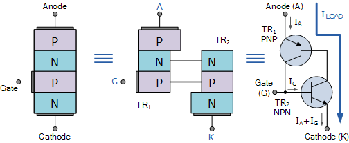
Que.71 What is thyristor? Give some examples of thyristors.
Answer:
- A thyristor is a power control device. i.e they can handle a large amount of power with a negligible amount of power consumption.
- It is a bistable device fabricated only with silicon.
- Ge thyristors are not practical.
- If a thyristor changes its state from off to on, because of applied voltage, it is called voltage operation.
- If a thyristor changes its state from off to on because of the applied current, it is called current operation.
- Example: SCR, DIAC, TRIAC
Que.72 What is SCR? What is its application?
Answer:
- It is a three-terminal power switching device having an anode-cathode and gate.
- Current in silicon controlled rectifier (SCR) is unidirectional, i.e. from anode to cathode.
- It works on the principle of current regeneration.
- It is a fast switch having a switching time of nanoseconds.
- In designing of SCR, the innermost layer is relatively lightly doped as compared to the outermost layer.
Applications of SCR:
- It is used in speed control of dc motor.
- Used in designing poly-phase rectifiers.
- Power supply inverter circuit.
Que.73 What is holding current and latching current in SCR?
Answer:
- Holding current: it is the minimum anode current that will hold the SCR in the state.
- Latching current: it is the minimum anode current required in the SCR so that SCR will continue to remain in the on state after removing the gate current.
- Note: In the conducting SCR, the holding current is always less than the latching current.
Que.74 What is a snubber circuit? Explain voltage and current snubber ckt.
Answer: The snubber circuit is used to protect the SCR against breakdown.
- voltage snubber circuit: it is used to protect the SCR against high dV/dt rating and it is done by connecting a resistor and capacitor in parallel with the SCR.
- current snubber circuit: it is used to protect the SCR against the high dI/dt rating by connecting the inductor in series with SCR.
Que.75 Which type of amplifier is best BJT or FET and why?
Answer: BJT amplifiers are most commonly used in comparison to FET amplifiers because the gain-bandwidth product of BJT is greater than the gain-bandwidth product of FET.
GO TO THE NEXT PAGE