Que.26 What is the relation between the mobility of the charge carrier and temperature?
Answer: Mobility of charge carriers decrease with temperature as a non-linear variation. As the temperature increases, the atoms in the material will vibrate and due to this thermal vibration, the movement of atoms is reduced, and hence the mobility of the charge carrier reduces.
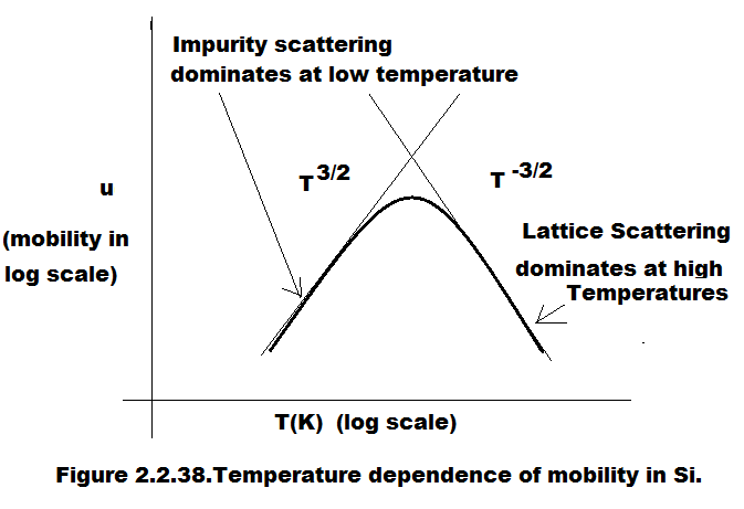
Que.27 What are the different scattering mechanisms in a semiconductor?
Answer:
- In a semiconductor, two different types of scattering mechanisms are used:
- Lattice scattering: mobility of electrons decreases as temperature increases as there are more collisions with lattice atoms that are vibrating.
- Surface scattering: this is also called impurity scattering, in this type of scattering mechanism, the mobility of electrons increases with temperature as a non-linear variation.
Que.28 what is an intrinsic semiconductor? The conductivity of intrinsic depends on what factor?
Answer:
- These are the pure semiconductors that behave as an insulator at 0K.
- At the temperature of 300K, covalent bonds between the atoms of a semiconductor start breaking, which creates electrons and holes. Electrons move from the valence band to the conduction band and holes remain in the valence band. These free particles generate current in the semiconductor. Si and Ge are examples of intrinsic semiconductors.
- Conductivity mainly depends on the
- Mobility of charge carrier: which depends on the temperature. With the increase in temperature, mobility decreases.
- Carrier concentration: with an increase in temperature, mobility decreases but the charge carrier increases due to a large number of covalent bonds breaking, which creates a large number of free electrons and holes.
- Hence, we can say the conductivity of an intrinsic semiconductor is mainly a function of temperature.
Que.29 What is Drift current in semiconductor devices? On what factors does it depend?
Answer: It is the flow of current through a material or device under the influence of an electric field.
- It depends upon the:
- Carrier concentration: with an increase in charge carriers, the conductivity of semiconductor material increases, hence drift current also increases.
- Mobility of charge carriers: same as carrier concentration, conductivity is directly proportional to the mobility of charge carriers.
- Electric field intensity
Que.30 What is thermally generated current?
Answer:
- Current generated in semiconductor material due to temperature only, known as thermally generated current or leakage current or minority carrier current.
- As this current depends on minority carriers and minority carrier concentration depends on temperature.
- For better performance of the device, this current must be as small as possible.
- Silicon has better thermal stability than Germanium.
Que.31 Definition of conduction sensitivity.
Answer: Variation of conductivity due to variation in temperature is called conduction sensitivity. The conduction sensitivity of Si is more than Ge.
Que.32 Why Silicon is mostly preferred as a semiconductor material?
Answer: Si is the most preferred semiconductor because:
- It has a smaller leakage current.
- It is suitable for low-power and high-power applications.
- It is available in plenty on the earth’s surface.
- It is the cheapest semiconductor.
- It has favorable properties to form SiO2, which is preferred in IC manufacturing.
Que.33 Why silicon is more efficient than germanium?
Answer: Si is considered more efficient than Ge because it has a high power handling capacity as compared to Ge and has a low leakage current.
Que.34 What are the common applications of semiconductor materials?
Answer:
- Temperature sensors are made with semiconductor devices.
- They are used in 3D printing machines.
- Used in microchips and self-driving cars.
- Used in calculators, solar plates, computers, and other electronic devices.
- Transistors and MOSFET used as a switch in Electrical Circuits are manufactured using semiconductors.
Que.35 What is Diffusion in semiconductor devices?
Answer:
- Diffusion is the process of migrating the charge carriers from high concentration to low concentrations or from higher density to lower density.
- Diffusion mainly occurs due to concentration gradient ie. due to unequal distribution of charge carriers.
- In a semiconductor, the carrier concentration is maximum on the surface of the semiconductor, and as we move into the depth of the semiconductor, carrier concentration decrease.

Que.36 What are the Applications of intrinsic semiconductors?
Answer:
- Silicon and germanium are the most common examples of intrinsic semiconductors. Both these semiconductors are most frequently used in the manufacturing of transistors, diodes, and other electronic components.
- PIN diode uses intrinsic semiconductors. Intrinsic SC is also used in microwave switches.
Que.37 What is a Hole in semiconductor devices?
Answer:
- The hole is basically an empty space created by an electron.
- It is defined as the deficiency of an electron in the broken covalent bond.
- It is a carrier of current with a positive charge of 1.6×10^-19 C.
- In conclusion, we can say that hole is not a particle and it does not exist. It is basically a valence electron assumed with a positive charge.
Que.38 What is Recombination in semiconductor devices?
Answer:
- The pairing of a free electron with a hole is known as the Recombination process.
- During recombination, free-electron fall from conduction to the valence band. ie. From high energy level to low energy level by releasing difference of this two energy in heat or light form.
- The free electron and hole will simultaneously disappear during recombination, and a covalent bond is created.

Que.39 What is Doping in semiconductors? Why doping is required in semiconductors?
Answer:
- It is the process of adding impurities to the semiconductor. The impurity atom that is added to the semiconductor is called dopants or impurity profile.
- This impurity profile will be maximum on the surface of semiconductors and gradually decrease into the depth of semiconductors.
- Doping in semiconductors is done to increase the carrier concentration, therefore, increasing the conductivity and also controlling the conductivity of the semiconductor as per requirement.
Que.40 What is the minimum doping required to convert intrinsic semiconductors to extrinsic semiconductors?
Answer: Minimum doping required to convert the intrinsic semiconductor to an extrinsic semiconductor is 1: 10^8
Que.41 What is the difference between direct band gap semiconductors and indirect band gap semiconductors?
Answer:
| Direct band gap SC | Indirect band gap SC |
|---|---|
| In this type, during recombination, most of the energy is released in the form of light. | During recombination, energy is released in the form of heat. |
| During recombination, most of the free electrons falling from the conduction band will collide with the crystal, the crystal will absorb energy from the falling electron and then get heated up. They now release energy in the form of heat. | During recombination, most of the free electrons falling from the conduction band will go to the intermediate level and then fall into the valence band, hence called as indirect band gap SC. |
| Electrons releases energy with or without a change in the momentum of electrons. | In this SC, the momentum of the falling electron must change due to the change in the velocity of falling electrons. |
| No change in the path of falling electrons | The path of electrons slightly changes. |
| Ex- GaAs, InP, CDs | Ex- Si, Ge |
Que.42 What is Extrinsic semiconductor? Give some examples.
Answer:
- Intrinsic semiconductors are doped to make an extrinsic semiconductor.
- Extrinsic semiconductors are divided into two categories as a result of doping:
- Atoms with an additional electron (n-type for negative, from group V)
- Atoms with one fewer electron (p-type for positive, from group III).
- Doping is the purposeful introduction of impurities into a very pure, or intrinsic, semiconductor in order to change its electrical characteristics. The kind of semiconductor determines the impurities. Extrinsic semiconductors are those that are light to moderately doped.
- Example- GaAs.

Que.43 What is Fermi energy in a semiconductor?
Answer:
- It is the maximum energy possessed by an electron at 0 kelvin or it is the maximum kinetic energy gained by an electron at 0 kelvin.
- It is also defined as the energy gained by the fastest-moving electron at 0 kelvin.
Que.44 What is compensated semiconductor?
Answer:
- It is an SC in which donor and acceptor impurities are added. When donor impurities are added into P-type or acceptor impurities are added into N-type, SC becomes a compensated semiconductor.
- When Nd> Na, a semiconductor is N-type compensated.
- When Na> Nd, a semiconductor is P-type compensated.
Que.45 What is the net charge on a semi-conductor?
Answer: Any semi-conductor which follows the law of electrical neutrality will always follow the law of conservation of charge. Hence, all semiconductors are electrically neutral.
Que.46 What is minority carrier injection?
Answer:
- Minority carrier injection: it is a process taking place at the boundary between p-type and n-type semiconductor materials, used in some types of transistors. Each semiconductor material contains two types of freely moving charges: electrons (negative charges) and holes (positive charges). Electrons are the more abundant, or majority, carrier in n-type materials, holes being the less abundant, or minority, carrier. In p-type materials, however, holes are the majority carrier, and electrons are the minority carrier. If a battery is properly connected to the semiconductor material, the p-type material may acquire additional electrons (minority carriers), injected into the p-type material from the n-type material by the flow of electrons from the battery. This is a minority carrier injection. It is important in bipolar junction transistors, which are made of two p–n junctions.
Que.47 What is the effect of doping on majority and minority carrier concentration?
Answer:
- In a semiconductor, doping increases the majority carrier concentration but it simultaneously reduces the minority carrier concentration.
- For example: In an N-type semiconductor, minority carriers are holes given by: p = Ni^2/Nd …..(i)
- So, it is clear that as Nd increases, minority carrier decreases.
Que.48 What is the effect of doping on the conductivity of extrinsic semiconductors?
Answer:
- As doping increases the carrier concentration by a large amount, hence conductivity in extrinsic semiconductors increases significantly.
- With 1:10^8 doping in Ge, conductivity increases 12 times, and with 1: 10^3 doping in Ge, conductivity increases 1200 times, which is significantly a huge increment.
- A highly doped semiconductor starts behaving as a conductor.
Que.49 What is a Degenerate semiconductor?
Answer:
- In an extrinsic semiconductor, a highly doped (1: 10^3) semiconductor exhibit some metallic properties, such as larger conductivity, NTC of semiconductor becomes PTC, bipolar nature of semiconductor becomes unipolar i.e. a highly doped semiconductor starts behaving as a conductor. Semiconductor with these properties is called degenerate semiconductors.
- Mass action law cannot be applied to this semiconductor. Degenerate semiconductors are often used in integrated circuits as a replacement for metal. Often superscript plus and minus symbols are used to denote relative doping concentration in semiconductors. For example, n+ denotes an n-type semiconductor with a high doping concentration. Similarly, p− would indicate a very lightly doped p-type material.
Que.50 How does temperature affect the conductivity of the extrinsic semiconductor?
Answer:

- At T = 0K , carrier concentrations are 0. Conductivity is zero and extrinsic SC will behave as an insulator.
- At 0K <T<300K, the conductivity of extrinsic semiconductors will be increasing with temperature due to ionization.
- At T= 300K, the conductivity of the Extrinsic semiconductor is maximum.
- At 300K <T<Tc, the majority carrier will become independent upon temperature and minority carriers will be increasing, mobility of charge carrier reduces with an increase in temp. hence conductivity starts decreasing.
- At Tc, i.e. at 400K also called curie temp. minority carriers’ approaches to majority carriers and extrinsic SC become intrinsic SC. Hence, conductivity will be minimum at this temp.
GO TO THE NEXT PAGE