In this article, we are going to learn about the Analog Electronics Interview Questions And Answers in a very detailed manner. This question we have covered is most important for interviews.
Analog Electronics Interview Questions
Que.1: What do you mean by operational Amplifier?
Answer: An operational amplifier is a direct-coupled, high-gain amplifier used for some mathematical operations such as addition, subtraction, multiplication, integration, differentiation, logarithmic operations, etc.
Que.2: List the ideal characteristics of an op-amp.
Answer:
- infinite voltage gain
- Infinite input resistance
- Zero output resistance
- Zero output offset voltage
- Zero input offset voltage
- Infinite bandwidth
- Infinite CMRR ( Common mode rejection ratio)
- infinite slew rate
Que.3: What are the main features of IC-741?
Answer:
- No external frequency compensation is required
- Short circuit protection
- offset null capability
- large common-mode and differential voltage range
- low power consumption
- No latch-up problem
Que.4: What is input offset voltage in op-amp?
Answer: Due to the non-linearity of the components in the circuits, there will be some output voltage available at op-amp even if the input voltage is not applied. So to null the output voltage at zero minimum input voltage is applied at the input of op-amp which is called input offset voltage. In short, the Minimum input voltage required to null the output voltage at zero is called input offset voltage.
Que.5: what do you mean by CMRR (Common mode rejection ratio)?
Answer: The significance of CMRR is the capability of the op-amp to reject the common-mode inputs available at the inverting and non-inverting terminal. Noise is the signal which is common at both the terminals of the op-amp. So in short CMRR is high, which means the op-amp capability is high to reject the noise signal so that it will not affect the output signal. CMRR is the ratio of the differential voltage gain to the common-mode voltage gain.
Que.6: Discuss the SVRR?
Answer: The full form of SVRR is the supply voltage rejection ratio. The change in an op-amp offset voltage caused by a variation in supply voltage is called the Supply voltage rejection ratio (SVRR).
Que.7: What is the Slew rate of an op-amp?
Answer: The slew rate is the maximum rate of change of output voltage per unit of time. The unit of slew rate is v/μs.
Que.8: Explain the effects of hysteresis.
Answer: It improves noise immunity. It reduces the response time. It reduces false triggering. When hysteresis increases then sensitivity reduces.
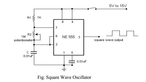
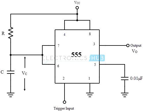
Que.9: Explain the timer IC-555.
Answer: IC-555 is a timer IC that is used in a stable multivibrator, square wave generator, triangular wave generator, pulse modulator, and pulse detector circuits.
Que.10: Explain IC.
Answer: An IC ( Integrated Circuit) is a miniature, low-cost electronic circuit consisting of active and passive components fabricated together on a single crystal of silicon. The active components are transistors, diodes, etc, and the passive components are resistors and capacitors.
Que.11: What are the advantages of ICs over discrete circuits?
Answer:
- Minimization & hence increases equipment density
- Cost reduction due to batch processing
- Increase system reliability
- Improved functional performance
- matched devices
- Increased operating speed
- Reduction in power consumption
Que.12: Process of fabricating ICs using planner technology.
Answer:
- Silicon wafer (substrate) preparation
- Epitaxial growth
- Oxidation
- Photolithography
- Diffusion
- Ion implantation
- Isolation technique
- metalization
- Assembly processing & Packaging
Que.13: List some linear applications of the op-amp.
Answer: Adder, Subtractor, Voltage-to-Current converter, Current to voltage converter, Instrumentation amplifier, Power amplifier, etc.
Que.14: List some non-linear applications of the op-amp.
Answer: Rectifier, Peak detector, Clipper, Clamper, Sample and Hold Circuit, Log amplifier, Anti-log amplifier, Multiplier, etc.
Que.15: What is Filter? Why filter is used?
Answer: A filter circuit is a device that converts the pulsating output of a rectifier into a steady-state DC level. It is essential to reduce the ripples from the pulsating DC supply available from rectifier circuits to the minimum to protect the load from damage. This is achieved by using a filter or smoothing circuit which removes the AC components and allows only DC components to reach the load. The filter circuit is always placed between the rectifier and the load.
Que.16: What are the commonly used types of filter circuits?
Answer: 1. Series Inductor Filter, 2. Shunt Capacitor Filter, 3. Choke Input Filter, 4. Capacitor input or Pie Filter
Que.17: What are the drawbacks of the series inductor and shunt capacitor filter?
Answer: A simple shunt capacitor filter reduces the ripple voltage but increases the diode current. The diode may get damaged due to the large current and at the same time, it causes greater heating of the supply transformer resulting in reduced efficiency. In an induction filter, the ripple factor increases with the increase in load resistance while in a capacitor filter, it varies inversely with the load. From the economic point of view, neither series inductor nor shunt capacitor types filter is suitable.
Que.18: What is Clipper?
Answer: In electronics, a clipper is a device designed to prevent the output of a circuit from exceeding a predetermined voltage level without distorting the remaining part of applied waveforms. Series clippers are employed as noise limiters in FM transmitters by clipping excessive noise peaks above a specified level.
Que.19: Application of Clippers.
Answer: It is used in television sets and FM receivers. It is also used for amplifiers and different types of opamps through which we can do some mathematical operations.
Que.20 What are oscillators?
Answer: Oscillators produce a waveform of the desired amplitude and frequency. They can take input from the output itself. For a complete oscillator circuit, we require a feedback device, amplifier, and feedback factor. Oscillators designed to produce a high-power AC output from a DC supply are usually called inverters.
Que.21 Why do we use the level shifter stage in op-amp?
Answer: The unbalanced output of the differential amplifier has DC in it which if passed to the output, may change the operating point or biasing conditions and result in distortions in output.
Que.22 Why do we use a compensation capacitor?
Answer: It is used to improve the stability of op-amp but it reduces the slew rate of op-amp because of the charging-discharging of the capacitor.
Que.23 Drawback of IC 741 op-amp.
Answer: Small slew rate which limits its application in high-frequency circuits.
Que.24 What is an instrumentation amplifier?
Answer: It is a circuit that converts changes in a physical process into amplifier voltages. It has a bridge network to detect changes in physical parameters followed by a voltage buffer and the differential amplifier.
Que. 25 Why op-amp is more used as an integrator but not as a differentiator?
Answer: In differentiator circuits, the high-frequency gain becomes too high so the circuit becomes unstable, and at high frequency, it provides amplification to noise frequency and noise also increases.
Also Read
👉🏻 Zener Diode
👉🏻 Photoconductive Cell | Photoresistor | Light Dependent Resistor
👉🏻 Tunnel Diode: Definition, Characteristics & Applications
Que. 26 Difference between Butterworth and Chebyshev filter.
Answer:
| Butterworth Filter | Chebyshev Filter |
|---|---|
| 1. This has a maximally flat passband. i.e. Gain remains constant inside the passband. | 1. Highest roll-off rate outside the passband. i.e. gain decreased at a higher rate. |
| 2. The width of the transition band is greater. | 2. Width if transition band is small. |
| 3. Butterworth filter poles lie on a circle. | 3. Poles lie in an ellipse. |
| 4. No. of poles are more, more components are required | 4. No. of poles is less so fewer components are required. |
Que. 27 Tell me something about the Schmitt triggers circuit.
Answer:
A circuit that converts any input to a square wave. Also called a regenerative comparator. It compares the input to predefine voltage levels V_{UT} & V_{LT} and produces output as either +Vsat or -Vsat.
Que.28 Application of Schmitt trigger.
Answer:
- It can be used to convert any signal to a square wave.
- To remove the chatter effect in the street light system.
Que.29 What is an oscillator?
Answer:
It is a circuit that provides sinusoidal output without giving any external input. It uses a positive feedback configuration.
Que.30 Why only positive feedback can provide oscillations?
Answer:
In -ve feedback, feedback signal will be added out of phase to input. so the net input reduces causing the output to reduce gradually and finally die out. But in +ve feedback, it is added in phase and if A\beta=1 maintained then it produces oscillations.
Que.31 What does an electronic circuit mean? Types of electronic circuits.
Answer: A circuit having at least one electronic device such as an amplifier, oscillator, etc. is known as an electronic circuit.
Types of the electronic circuit:
- Analog circuit: a circuit that can process analog signals or a ckt whose o/p and i/p are analog signals. Example- amplifier, rectifier, etc.
- Digital circuit: a circuit that processes digital s/g or signals which are in the form of 0 & 1. Example- adder, shift register, etc.
- Mixed-signal circuit: which uses both analog and digital circuits. Example- analog to digital converter and digital to analog converter.
Que.32 What is a power supply? What is a regulated power supply? What are the components of the power supply?
Answer:
- An electronic system that converts AC power into DC power is known as a power supply system.
- A regulated power supply means output remains constant even if input changes.
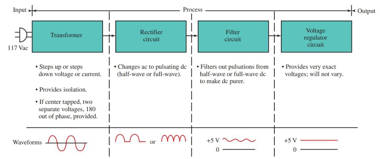
The components of power supply are:
- Rectifier: which converts pure AC signal to pulsating DC signal (AC+DC).
- Filters: which convert pulsating DC signal to fluctuating DC signal.
- Voltage regulator: which finally converts fluctuating DC to stable or regulated DC.
Que.33 What is the regulation factor in analog circuits? What should be its ideal value? Types of regulation.
Answer: It is the measure of change in DC output voltage due to a change in load current.
%Regulation=\frac{V_{DCNL}- V_{DCFL}}{V_{DCFL}}
- Ideally regulation factor should be 0 i.e. DC output voltage should not change with change in load current.
Types of regulation:
- Line regulation: refers to keeping output voltage constant irrespective of change in AC supply voltage. i.e. in this case load current is kept constant.
- Load regulation: it is the process of keeping output voltage constant irrespective of variation in load current. i.e. input voltage is kept constant.
Que.34 What is peak inverse voltage? Why high PIV is undesired?
Answer:
- It is the maximum voltage that appears across a diode when it is a reverse bias state or non-conduction state in a rectifier.
- For safe operation of the diode, PIV should be less than the breakdown voltage.
- Higher PIV is undesired because it will require a higher breakdown voltage, which will be costlier.
Que.35 Define filters in the power supply. Types of filters used in power supply.
Answer:
- Filters are frequency-selective network, which passes a desired range of frequencies but eliminates unwanted frequencies. In the power supply, it is used to remove the unwanted AC component, which is present in the output of the rectifier.
- Filters in power supply consist of large capacitors( micro to milli farad) and large inductors( of a few henries).
Filters used in power supplies are:
- Capacitive filters
- Inductive filter
- LC or L section filter
- Inductor filter
- C-L-C or pie section filter
Que.36 What is a Voltage regulator? and what types of voltage regulators?
Answer:
- Voltage regulator: A circuit that maintains the DC output voltage of a power supply irrespective of fluctuations in AC supply and variation in load current.
- Types of voltage regulators:
- Linear regulator: IC regulators – these are IC regulators in which the transistor operates in the linear or active region.
It includes: Fixed voltage IC regulator- 78XX, 79XX , Adjustable voltage regulator- IC-723
Regulator using direct components – 1. Shunt type 2. Series type
- Nonlinear regulator or switching regulator: in this type, the transistor is operated in a cut-off or saturation region.
Que.37 Working of Zener diode-based regulator.
Answer:
- A Zener diode is used which is connected in parallel with a load resistor, hence also known as a shunt regulator.

Here,
Rs: resistance is used to prevent the heavy flow of current flow through the Zener diode.
Vs: the unregulated supply voltage.
Iz: Zener current
IL: load current
I_S=\frac{(V_S - V_Z)}{R_S}…… KVL
I_S=I_Z+I_L …… KCL
- For proper operation, the current through Rs should be at least equal to the sum of the knee current and specified load current.
i.e. I_S\geq I_{Zmin} + I_L
- and for the safe operation of the zener diode,
I_S\leq I_{Zmax} + I_L
Note: In a Zener diode shunt regulator, the maximum value of Rs is obtained by considering the minimum value of supply voltage and minimum Zener current, and the minimum value of Rs is calculated by considering the maximum supply voltage and maximum Zener current.
Que.38 Disadvantage of Zener diode regulator.
Answer:
- The output voltage can vary with temperature as the Zener diode is temp. Dependent.
- A large change in load current cause a much change in Zener current and thereby output voltage may have considerable change.
Que.39 What are the Wave shaping circuits. Application of waveshaping circuits.
Answer:
- Circuits are responsible for changing the shape of the alternating waveforms.
- There are basically two types:
1. Linear wave shaping circuits: it is performed by linear elements such as R, L, and C.
Example- low pass RC and High pass RC circuits.
2. Non-linear circuits: it is performed using non-linear elements such as diodes.
Example- clippers: it is a non-linear waveshaping ckt. which can remove or cut the unwanted portion of a signal.
Application of waveshaping circuits:
- Clipper can be used to limit the amplitude of a signal, hence also called amplitude limiter.
- It can be used to eliminate the noise from pulse waveforms in digital communications.
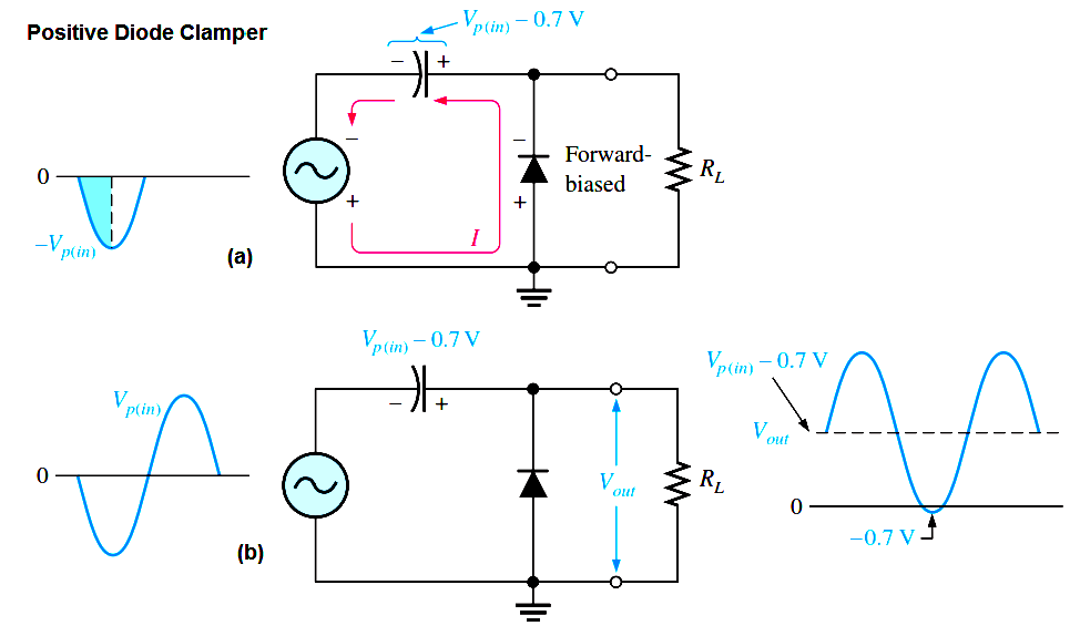
Que.40 What is clamper and its application?
Answer:
- Clamper is also called a DC restorer or DC reinserted as it is responsible for adding DC voltage to an AC waveform.
- It does not change the shape of the signal instead it shifts the signal in either an upward or downward direction.
- DC restorer because it can restore the DC voltage level of a signal which has lost its DC value in electronic processing.
Que.41 What is the significance of form factor in rectifiers?
Answer:
- The form factor is given by the formula,
Form\; Factor=\frac{I_{rms}}{I_{DC}}
- It is the ratio of the RMS value of alternating current and DC current.
- It basically signifies the greater smoothness in the waveform or less ripple factor.
Que.42 Why BJT is called a current controlled device?
Answer:
- In a BJT, base current Ib is nearly the same as recombination current, which is provided by biasing supply.
- If the supply of compensating electrons is increased then the base region becomes negative due to a surplus of electrons and it attracts a greater no. of holes from the emitter, therefore the flow of holes from emitter to collector increases, if the supply of compensating electrons is reduced, then base become positive due to electron deficiency and it attracts large no of the hole from the emitter, therefore, the flow of electron from emitter to collector decreases.
- Thus, it implies the supply of compensating electron or base current Ib controls the flow of current from emitter to collector, hence BJT is called a current-controlled device.
Que.43 Why emitter is heavily doped and the collector moderately doped in BJT?
Answer:
- In a BJT, an emitter is a region that emits the majority of carriers. It is heavily doped so that it can emit large no. of carriers.
- While collector is moderately doped because if it is lightly doped, its conductivity becomes low and if it is heavily doped, the breakdown voltage of the collector junction becomes smaller, therefore to achieve better conductivity and higher breakdown voltage, the collector is moderately doped.
Que.44 What is the early effect or base width modulation in BJT? What are its consequences?
Answer:
- It refers to the decrease in effective base width due to a decrease in reverse bias voltage across the collector junction.
- The early effect has three consequences:
- Large signal current (alpha) increase- as Vcb increases effective base width decrease which implies a decrease in no. of recombination or increase in collector current, hence alpha increases.
- For small increases in alpha, beta(small-signal current gain) increases by a large amount.
- Emitter current Ie increases due to an increase in hole concentration gradient.
Que.45 What is punch through effect?
Answer:
- At a large value of reverse bias at the collector junction, the depletion region fully occupies the base and the effective base width becomes zero. This is called the punch-through effect.
- When the punch-through effect occurs, the collector and emitter get electrically short-circuited. As the collector is at a strong negative potential, a large no. of holes travel from emitter to collector i.e. heavy current flow which can damage BJT.
Que.46 What factors are responsible for instability in collector current? What are its consequences?
Answer: Factors responsible for instability in collector current,
\boxed{I_C=\beta_F I_B + I_{CEO} \approx \beta_F I_B}
- Variation in Ico: Ico is the reverse saturation current of the collector junction and it is temperature-dependent. By 1 degree rise in temp. Ico has increased by 7%. A change in Ico will cause a change in Ic.
- Variation in VBE: VBE is the forward voltage of the emitter junction, it is also temp. Dependent. By a 1 degree rise in temp, it increased by 2.5mV. A change in VBE will cause a change in IB, hence the IC change.
- Variation in \beta: \beta is common-emitter current gain, it can vary due to transistor replacement or due to changes in temp.
This instability in Ic has two undesired effects:
- The operating point does not remain at the center of the load line, which can cause distortion in the output signal.
- A thermal runaway can occur which damages a BJT.
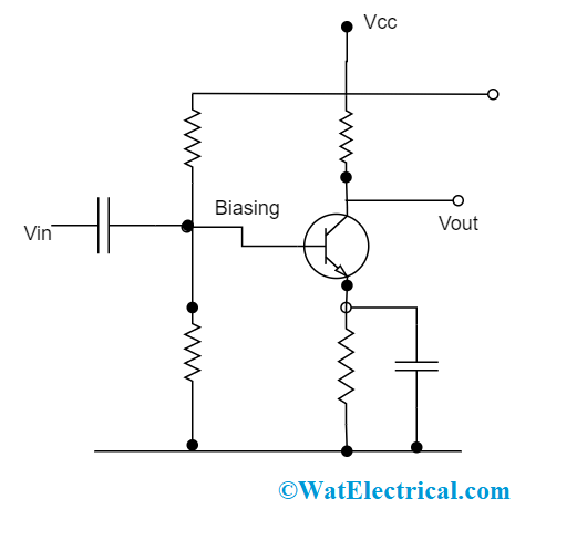
Que.47 What is biasing? What are the different biasing circuits used for operating BJT as amplifiers?
Answer:
- Biasing refers to providing DC current & DC voltage to an electronic device so that the device works as desired.
- A BJT is biased to operate in an active region so that it can be used as an amplifier.
BJT biasing circuits to operate it as an amplifier are-
- Fixed bias ckt
- Collector to base bias ckt.
- Self-bias ckt.
Que.48 What is a thermal runaway condition? How it can be avoided?
Answer:
- It is the process of self-destruction or self-damage of BJT, because of overheating at the collector junction due to an increase in collector current with an increase in Ico. If the temperature increases reverse saturation current causes collector current hence power dissipation increases at collector junction which increases heat produced at collector junction implying an increase in temperature. This is a thermal runaway. It occurs mostly in power amplifiers.
Condition to prevent thermal runaway:
- Thermal runaway can be avoided if the rate at which heat is produced at the collector junction is less than the rate at which heat is transferred or dissipated to the surroundings.
- If VCE <= Vcc/2, then thermal runaway does not occur irrespective of the value of theta, Such a circuit is called a thermally stable circuit.
- If VCE > Vcc/2, then thermal runaway can be avoided.
Que.49 How BJT can act as an amplifier?
Answer:
- The amplifier is basically an electronic ckt. which increases the strength (power level) of a weak electronic signal without a change in its shape.
- BJT is able to act as an amplifier because of small change in voltage at the input terminal can cause a large change in voltage at the output terminal
Que.50 What are the advantages of BJT over MOSFET?
Answer:
Advantage of BJT over MOSFET:
- BJT has higher transconductance therefore gain-bandwidth product is greater in BJT than in JFET & MOSFET, hence BJT is preferred in high-frequency amplifiers.
- BJT has higher fidelity & better gain in the linear areas as evaluated with the MOSFETs.
- As compared to MOSFETs, BJTs are very faster because of low capacitances on the control pin.
- BJTs are a very good choice for voltage and low-power applications.
Que.51 Which is a better amplifier BJT or MOSFET?
Answer:
- Both the BJT and MOSFET include unique features and their own advantages and disadvantages. But, we cannot say which is good in BJT & MOSFET as the matter is extremely subjective. But before selecting the BJT or MOSFET, there are several factors that need to consider like the level of power, efficiency, drive voltage, price, speed of switching, etc. Usually, a MOSFET is used in power supplies more efficiently because the working of MOSFET is faster due to metal oxide usage apart from BJT. Here, BJT depends on the combination of electron-hole.
- MOSFET works with low power once switching at high frequency because it has a quick switching speed so it leads through grid-oxide controlled field effect but not through the recombination of an electron or hole like BJT. In MOSFET, the circuit-like gate control is much simpler
- There are numerous reasons that stand out:
Fewer Conduction Losses
- A bipolar junction transistor includes a stable saturation voltage drop like 0.7 V, whereas the MOSFET includes a 0.001-ohm on-resistance that leads to fewer power losses.
High Input Impedance
- A bipolar junction transistor uses a low base current for operating a larger collector current. And they perform like a current amplifier. The MOSFET is a voltage-controlled device and it doesn’t include gate current almost. The gate works like a value capacitor and it is a significant benefit in the applications of switching & high current because the gain of the power BJTs has medium to low, which needs high base currents to produce high currents.
- The area occupied by the MOSFET is less as compared with BJT like 1/5th. The BJT operation is not as simple as compared with MOSFET. So FET can be designed very easily and can be used like passive elements instead of amplifiers.
Que.52 How is BJT biased in integrated circuits?
Answer:
- BJT is biased in IC amplifiers by using a special circuit known as a current mirror.
- Current mirror- here two identical transistors have a large beta in which the collector of one transistor is shorted to its base, i.e. VCB = 0 or VCE = VBE therefore Q1 transistor will remain in the active region, and it will never enter saturation.

- For the two transistors, bases are short and emitters are grounded, therefore,
VBE1 = VBE2
i.e., IB1 = IB2
- hence, for an equal value of \beta, IC1 = IC2
I_{in}=I_C+I_B+I_B
I_{in}=I_C+2I_B
I_{in}=I_C+2 \left ( \frac{I_C}{\beta} \right)
I_{in}=I_C\left ( 1+ \frac{2}{\beta} \right)
\boxed{I_C=\frac{I_{in}}{\left(1+\frac{2}{\beta} \right)}}
Que.53 What are the applications of current mirror circuits?
Answer:
Application of current mirror circuits:
- A current mirror is used as a constant current source to bias the BJT in IC amplifiers.
- A current mirror is used as an active load in ICs amplifiers to obtain higher voltage gain.
Que.54 What are the different compensation methods to keep the IC stable?
Answer: It is a method of keeping Ic stable by connecting temperature-dependent devices such as diodes, thermistors, and sensors.
Que.55 What is a buffer circuit? How does BJT act as a buffer circuit?
Answer:
- Buffer circuit: A circuit that is used for impedance matching between source and load circuits. So that maximum power is transferred from the source to the load circuit.
- A common-collector amplifier in BJT is used as a voltage buffer between source and load as it has large input resistance, smaller output resistance, and unity voltage gain.
- The common base amplifier in BJT is used as a current buffer between source and load as it has smaller input resistance, large output resistance, and unity current gain.
Que.56 What are the advantages and applications of RC-coupled amplifiers?
Answer:
- Advantages of RC coupled amplifier:
- It has a better frequency response.
- DC isolation between amplifier and load.
- Application: it is used to amplify the audio and video frequency signal.
Que.57 How are BJT amplifiers classified?
Answer:
- On the basis of the interconnection of amplifier and load, BJT amplifiers are divided into three types:
- RC coupled amplifier:
- Direct-coupled amplifier: voltage gain does not decrease at low frequencies because of large capacitors but voltage gain reduces at high frequencies due to junction capacitances.
- Transformer coupled amplifier: voltage gain decreases at low frequencies due to the inductance of primary and secondary windings. A peak appears in frequency response because of leakage capacitances and inductances.
Que.58 Advantage, disadvantage, and application of direct-coupled amplifier.
Answer:
Advantages of direct-coupled amplifier:
- It can amplify DC signals also.
- It is ideal for fabrication on silicon chips as it does not have large capacitances.
- All IC amplifiers are direct-coupled amplifiers.
The disadvantage of direct-coupled amplifier:
- Maximum power cannot be transferred to the load due to impedance mismatch.
- No DC isolation, which causes disturbance in the biasing condition of the amplifier.
Application of direct-coupled amplifier:
- It is used as a DC amplifier and very low-frequency amplifier as it can amplify frequency signals of 1hz or 2hz.
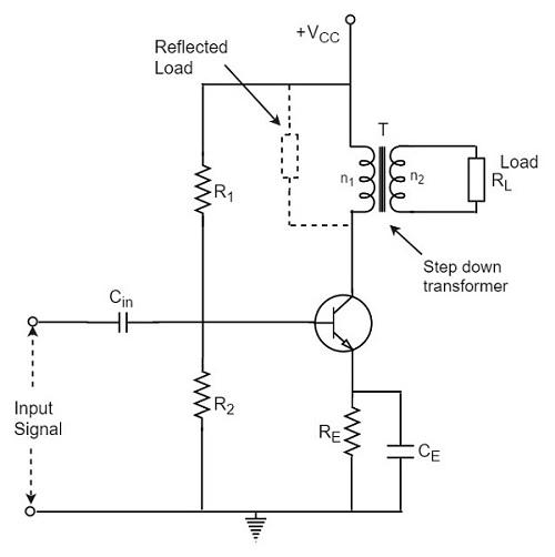
Que.59 Advantage, disadvantage, and application of transformer-coupled amplifier.
Answer:
Advantages of transformer-coupled amplifier:
- Maximum power can be transferred to the load due to the impedence-matching property of the transformer.
- Dc isolation between amplifier and load.
- Better efficiency because primary winding does not dissipate DC power.
- Higher voltage gain than RC coupled amplifier, if turns ratio, is greater than 2.
The disadvantage of transformer-coupled amplifier:
- Improper frequency response.
- The transformer is bigger in size and costlier.
Application of transformer-coupled amplifier:
- These are used in power amplifiers.
Que.60 What is a MOSFET? Why MOSFET is a voltage-controlled device.
Answer:
- MOSFET refers to a metal oxide field effect transistor which is also called voltage controlled capacitor, as a parallel plate is formed at the gate region, with an aluminum plate and semiconductor channel acting as two plates of a capacitor and SiO2 act as the dielectric.
- MOSFETs, can either be of depletion type or enhancement type. depletion type is when a transistor conducts current across the drain-source terminal in the absence of voltage to the gate terminal. Enhancement-type transistors are transistors that conduct current across the source-drain region only if the voltage is applied to the gate terminal. In the absence of voltage to the gate terminal in an enhancement-type transistor, the transistor will not conduct current across the drain-source region. Only if sufficient voltage is applied to the gate terminal of a transistor for an enhancement type transistor will it conduct current across the drain-source region.
- It is called a voltage control device because a small change in the gate to source voltage Vgs causes a proportionate change in drain current. However it acts as a constant current source with respect to Vds in the saturation region.
Que.61 What is JFET? How does it differ from MOSFET?
Answer:
- JFET refers to the junction field-effect transistor. The operation of the device depends on the electric field intensity produced in the channel. When 0V is fed into the gate of a JFET along with proper biasing to the source and drain terminals, the JFET operates at full conduction. Applying voltage to the gate terminal of JFET makes it more resistive and less current flows. Once the voltage reaches a certain threshold, all current flow from the source-drain terminal ceases.
Difference between JFET and MOSFET:
| JFET | MOSFET |
|---|---|
| JFET is a discrete three-terminal device. (source, gate, and drain). | It is called an insulated field effect transistor having 4 terminals. ( source, gate, drain, and substrate). |
| Size more than MOSFET. | Smaller in size than JFET. |
| Not easy to fabricate. | Easier to fabricate than JFET. |
| Slower than MOSFET. | MOSFET is faster than JFET. |
| JFET is always operated under depletion mode. | MOSFET operates in depletion as well as enhancement mode. |
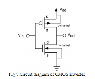
Que.62 How does the CMOS inverter work as a NOT gate?
Answer:
- CMOS inverter is used as NOT gate in digital circuits. When the input voltage is logic 1 or 0.
- When the input voltage is logic 1 or Vdd-
Vgsn=Vdd …… which implies NMOS on.
Vsgp = 0 …………. which implies PMOS off
- When the input is logic 0 then-
Vgsn = 0 … implies NMOS off
Vsgp = Vdd …. implies PMOS on
Hence, Vo = Vdd
Que.63 What is a Darlington amplifier? Application of Darlington amplifier.
Answer:
- Darlington amplifier: it is a cascade of two common collector amplifiers or cascade of two common drain amplifiers. It has very high input resistance, low output resistance, unity voltage gain, and high current gain.
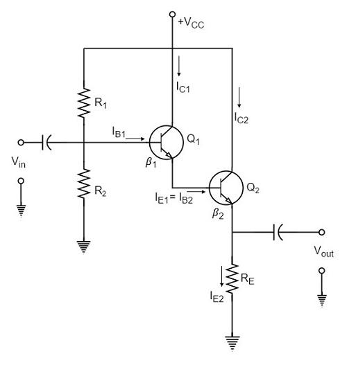
- Application: it is used as a voltage buffer for impedance matching.
Que.64 What is bootstrap biasing?
Answer:
- It is a special biasing ckt. which is used in the Darlington amplifier to prevent the decrease in input resistance. If self-bias ckt. is used, then input resistance decreases due to biasing resistors R1 and R2, to prevent this, we use bootstrap biasing ckt. which uses a large capacitor(microfarad) in between two resistors R1 and R2.
Que.65 What is a Cascode Amplifier? Application of the same.
Answer:
- It is a cascade of a common emitter and a common base amplifier.
- Its main feature is, that it has large bandwidth, therefore it is used as a wideband amplifier to amplify video frequency signals.
Que.66 What is a tuned amplifier? Application of tuned amplifier circuit.
Answer:
- It is a narrow-band amplifier that uses a parallel LC circuit as a load. Its main application is in radio frequency amplifiers.
- In this type of amplifier, voltage gain is varied with frequency and becomes maximum at a frequency of resonance. Narrow bandwidth is achieved using a parallel LC circuit having a large quality factor.


- Application: In a superheterodyne receiver single tuned amplifier is used as an RF amplifier and a double-tuned amplifier is used as an IF amplifier.
Que.67 What type of distortion occurs in amplifiers?
Answer:
Distortion in amplifier: If the output signal does not resemble an input signal, then the output is said to be distorted.
Distortion in amplifiers is of three types:
- Harmonic distortion: occurs in large-signal amplifiers or power amplifiers due to the non-linearity of the transistor. Nonlinearity causes harmonic frequencies in the output signal. Thus the appearance of harmonic frequencies in the output signal is known as harmonic distortion.
- Frequency distortion: refers to providing unequal amplification to different frequencies present in the input signal. Frequency distortion occurs due to the presence of reactive elements such as inductors and capacitors.
Example: RC coupled amplifier provides unequal amplification of different frequencies.
- Phase shift or delay distortion: refers to providing unequal phase shift to different frequencies present in the input signal. It also occurs due to reactive elements.
Que.68 Why do we use negative feedback in an amplifier?
Answer: In a basic amplifier (without feedback) gain is unstable due to variation in device parameters with temperature and time.
So negative feedback is used:
- To make the gain stable against variation in device parameters.
- To reduce all types of distortions in amplifiers
- To obtain desired values of input and output resistances.
Que.69 What are the effects of negative feedback on the various characteristics of amplifiers?
Answer: Effect of negative feedback on characteristics of the amplifier:
- Effect on gain: negative feedback decreases the overall gain.
- Effect on cut-off frequencies: negative feedback decreases the lower cut-off frequencies and increases the higher cut-off frequencies.
- Effect on the stability: it decreases the sensitivity of gain towards device parameters.
- Effect on frequency distortion: when negative feedback is used, bandwidth increases, therefore gain remains constant over a wide range of frequencies, hence amplifier is able to provide a uniform amplification over a wide range of frequencies.
- Effect on harmonic distortion: negative feedback reduces harmonic distortion by decreasing the non-linearity of the transistor.
Que.70 What is a power amplifier? Where do we use the power amplifier?
Answer:
- Power amplifier: it is a large signal amplifier. The power amplifier uses a power transistor that operates at a greater voltage (VCE of more than 10V) and a collector current of a few amperes. It supplies large AC output power because it internally converts a part of DC power obtained from the biasing supply into AC power.
- Application: A power amplifier is used at the final stage or output stage in a multi-stage amplifier.
Que.71 What are the advantages of using a Class A power amplifier? Where do we use the class A amplifier?
Answer:
- Advantage of using a class A amplifier is that we keep the operating point at the center of the load line, hence the output is undistorted.
- Class A amplifier is mostly used as a small-signal amplifier or voltage amplifier because it provides undistorted output. It is also used in high-frequency audio systems as an audio frequency power amplifier.
Que.72 What is a complementary push-pull amplifier? What are the disadvantages of push-pull amplifiers?
Answer: A complimentary push-pull amplifier consists of a pair of complementary transistor i.e. NPN and PNP transistor having identical characteristics.
- During the positive cycle of input, the NPN transistor conducts and pushes the current through load resistor R.
- During the negative cycle, the PNP transistor conducts and pulls the current out of the load resistor.

- It is suitable for ICs(integrated circuits) as it does not require any transformer.
Disadvantages of push-pull amplifier:
- Two biasing supplies are required, hence it is difficult to get two complimentary transistors with identical chars.
- Maximum power transfer to the load is not possible.
Que.73 Define Active filter. What is the difference between active and passive filters?
Answer: A filter consisting of R, and C elements and an active device such as opamp, FET, and BJT is called an active filter.
| Active filter | Passive filter |
|---|---|
| It consists of R and C elements along with an active device. | It consists of passive elements such as R, L, and C only. |
| It provides filtering as well as amplification. | It provides only filtering. |
| Used as audio frequency amplifier. | It is used at high frequency or radio frequency. |
Que.74 What is the application of the sample and hold circuit?
Answer: It is used in analog to digital converters.
- it consists of two voltage followers: an input voltage follower and an output voltage follower, a MOS switch, and a low leakage capacitor.
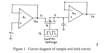
- When Vcontrol is logic 1, the MOSFET switch turns on and capacitor voltage follows input voltage. This is called a sampling operation.
- When Vcontrol is logic 0, the MOSFET switch turns off and capacitor voltage remains constant because the output follower does not allow to discharge, this is called hold operation.
Que.75 What is a voltage follower circuit? What is the application of voltage follower?
Answer:
- Voltage follower circuit: A circuit in which output follows the input voltage due to a physical short circuit. It is also called a unity gain non-inverting amplifier.

Application of voltage follower:
- It is used for impedence matching.
- It is used in the sample and hold circuit.
- It is used in instrumentation amplifiers.
- It is used in 1st-order Butterworth filters.
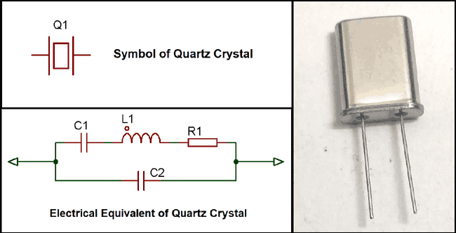
Que.76 What is a Crystal oscillator? What is the application of a crystal oscillator?
Answer: It is an LC oscillator in which a quartz crystal is used in place of the inductor.
- Quartz is a piezoelectric material that converts energy from electrical to mechanical and mechanical to electrical. The circuit diagram includes R, L, and C as components of quartz material in parallel with a capacitor.
Application of crystal oscillator:
- Crystal oscillators are used when a stable frequency is needed such as to generate a clock signal for the microprocessor.
- All electronic watches use a crystal oscillator.
Que.77 Where do we use the Hartley oscillator?
Answer: The Hartley oscillator is used as a voltage-controlled oscillator or FM generator if a varactor diode is used in place of the capacitor.
Que. 78 What is the difference between a waveform generator circuit and an oscillator circuit
Answer:
- Waveform generator circuit: A circuit that generates non-sinusoidal output such as square wave, triangular wave, etc. is known as a waveform generator.
- Oscillator Circuit: A circuit that generates an AC waveform without using AC input is called an oscillator. Oscillators generate sinusoidal output.
Que.79 How does a ramp generator circuit work?
Answer:
- Ramp generator circuit: As the name suggests, ramp generator circuits generate a ramp waveform or sawtooth waveform.
- The sawtooth waveform consists of a voltage that increases linearly with time until it reaches a predetermined final value, instantaneously returns to zero, and immediately increases again as the cycle repeat again.
- It can be generated by using an IC-555 timer circuit, in which a constant current source is used in place of the resistor.
- When the constant current source is used, the charging current of the capacitor remains constant, and thereby capacitor voltage increases linearly and the ramp signal is generated.
Que.80 Types of audio-frequency amplifiers and their application.
Answer: Audio frequency oscillator circuits are used in the audio systems to generate audible sound. For example, doorbells, and alarm systems.
There are two types of audio frequency oscillators:
- Wein bridge oscillator: it consist of a noninverting amplifier that provides zero phase shift and an RC feedback network that also provides zero phase shift. Hence phase shift remains zero and oscillation occurs at frequency fo. These are mostly used for audio testing.
- RC phase shift oscillator: which can be made using either BJT, FET, or OP-AMP. These oscillators are used in musical instruments, GPS units, and voice synthesis.
Que.81 Voltage to frequency converter circuit.
Answer:
- It is an oscillator circuit whose frequency is linearly proportional to the control voltage.
- When in an IC-555 astable multivibrator circuit, a control voltage is applied at the control pin, and the circuit acts as a voltage-controlled oscillator or voltage-to-frequency converter.
Que. 82 Why two differential amplifiers are used in the internal structure of IC-741?
Answer: Two differential amplifiers are used in the internal structure of op-amp IC-741 to obtain high voltage and high CMRR.
Que.83 Why opamp is used in the analog system over BJT and FET?
Answer: Opamp is preferred in analog systems over BJT and FET because circuit design becomes easier with an opamp circuit.
Que. 84 What is a differential amplifier? What are the different modes of operation of the differential amplifier?
Answer:
- Differential amplifier: A circuit that amplifies the difference between two input voltages.
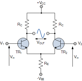
- A differential amplifier can be used in 4 different modes:
- Dual input balanced output- it is also called fully differential mode.
- Dual input unbalanced output mode or semi-differential mode.
- Single input balanced output
- Single input unbalanced output
Que. 85 What is a level shifter circuit? Where do we use a level shifter circuit?
Answer:
- It is a circuit that shifts the DC voltage level of a signal to 0 volts.
- It is the opposite of clamper. it is basically a common collector circuit that has unity voltage gain, high input resistance, and low output resistance.
- It is designed to eliminate a particular DC voltage.

- It is mainly used in the internal structure of opamp to prevent the loading effect and to eliminate the undesired DC signal.
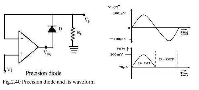
Que. 86 What is a precision diode or super diode? Application of the same.
Answer:
- It is the interconnection of an op-amp and a normal diode. It is equivalent to the ideal diode.
- When the input signal lies in milli or microvolt, then a precision diode is used for signal processing such as clipping and rectification.
- Precision diodes are used for half-wave and full-wave rectification of AC signals using opamp.
Que. 87 What is a delay equalizer circuit?
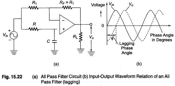
Answer: All pass filter passes all frequencies but provide different phase shifts to each frequency, it is used for phase equalization or delay equalization in a communication system. Hence also known as a delay equalizer.
Que. 88 What is the role of the input follower and output follower circuit used in the sample and hold circuit?
Answer: An input follower in the sample and hold circuit is used to eliminate the effect of source resistance whereas an output follower is used to prevent the discharging of the capacitor during the hold interval.
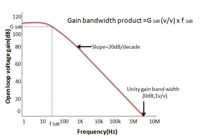
Que. 89 What is unity-gain bandwidth in an opamp?
Answer:
- Unity gain bandwidth (UGB): is a frequency at which the open-loop gain of op-amp becomes unity. It is also called a gain-bandwidth product of opamp. It is the highest frequency up to which op-amp can provide amplification.
Que. 90 What is the Schmitt trigger oscillator?
Answer:
- An astable multivibrator is equivalent to a Schmitt trigger with an additional RC network, hence called a Schmitt trigger oscillator.
- It is a circuit whose output does not have any stable state. Output has two quasi-stable states, and output keeps toggling between these two states without any external input. Hence it generates a square waveform. So this circuit is also known as a square waveform generator or free-running oscillator.
Que.91 What is a monostable multivibrator?
Answer:
- It is a circuit whose output has one stable state and one quasi-stable state, if external input is not applied then it remains in the stable state forever.
- If the trigger input is applied, then the output goes into a quasi-stable state but again returns to a stable state after a short duration of time. Thus a monostable ckt. generates pulse output when the trigger is applied.
Que.92 What is the diode-connected MOSFET?
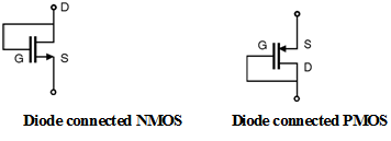
Answer: When the drain is shorted to the gate, then MOSFET will always be in the saturation region, this is called diode-connected MOSFET. It is used as an active load in IC MOS amplifiers.
Que. 93 What is a pass transistor?
Answer:
- It is a MOSFET used as a switch to pass logic levels between nodes of a circuit instead of a switch connected directly to a supply voltage.
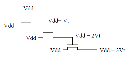
- When the gate voltage is equal to (source) input voltage, switch ON and the output becomes equal to (Vdd – Vt).
- When the input voltage is zero, the output voltage is zero. The switch is OFF.
Que.94 How BJT can be used as a switch?
Answer:
- When we operate BJT as a switch, it must be operated in such a way that power loss during ON and OFF should be nearly zero or very low.
- To operate BJT as a switch, it can be operated in cut-off and saturation regions.
- In the cut-off region: the base current is nearly zero, hence Ic (collector current) has a very small constant value for a wide range of Vce( collector to emitter voltage), hence power loss across the transistor is ( Ic*VCE) is negligible. So, in the cut-off region, BJT act as an OFF switch as the transistor act as an open circuit, and the entire open-circuit voltage appear across the load.
- In saturation region: base current becomes much higher than collector current or we can say IB > IC, and Vce becomes less than or equal to 0.2, then again the power loss across transistor becomes negligible. Here transistor behaves ON switch because the entire load current flow through the transistor.
Que.95 What are the advantages of the self-bias circuit in BJT over fixed bias and collector to base bias?
Answer:
Advantage of the self-bias circuit:
- Least stability factor or better stability in Ic.
- The stability factor is independent of load resistance.
- It can be used in all three configurations of BJT, while fixed bias and collector-to-base bias are appropriate only for common emitter configuration
Que.96 When do the virtual short ckt and virtual ground concepts fail in opamp?
Answer: When opamp enters saturation, the concept of virtual ground and virtual short circuit fails. Because this concept is applicable to negative feedback opamp circuits. which has linear characteristics and when opamp enters saturation, it becomes a positive feedback circuit, and the concept of linearity is not applicable in this case output saturates to a particular voltage.
Que.97 When compensation resistors are used in an op-amp circuit?
Answer:
- When the opamp has a non-zero input bias current, then the amplifier generates a non-zero output for zero input, the output voltage is called output offset voltage.
- In order to make this offset zero, compensation resistors are required in the inverting amplifier as this offset is negligible in the case of the non-inverting amplifier.
- This resistor is connected to the non-inverting node and its value should be equal to the value of the parallel combination of all the resistors at inverting node.
Que.98 How can you design a current-to-voltage converter using an op-amp circuit? Application of the same.
Answer:
- The current-to-voltage converter is used to convert the output current of a transducer into proportionate voltage. It is also called a trans-resistance amplifier.
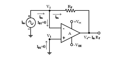
- Example: Photodiode uses an I-to-V converter.
Que.99 What is the purpose of using a shunt capacitor in a BJT amplifier?
Answer: The shunt capacitor in the BJT amplifier is used to limit the bandwidth of amplifier as bandwidth is inversely related to the shunt capacitor.
Que.100 What is a microwave amplifier?
Answer: It is the amplifier used in cellular communication and microwave communication. It amplifies frequencies that lie in GHz, which are microwave signals.
This list is incredibly helpful! I’ve been preparing for interviews and these questions cover a wide range of topics in analog electronics. Thanks for compiling such a resourceful post!
This post is incredibly helpful for anyone preparing for electronics interviews! The questions are relevant and comprehensive. I especially appreciated the clear explanations in the answers. Great job compiling this resource!
This post is incredibly helpful! The depth of questions and clear answers really prepares me for my upcoming interviews. Thanks for putting this together!
This list is incredibly helpful for anyone preparing for analog electronics interviews! I especially appreciate how the questions are categorized by difficulty. It really makes the preparation process feel more manageable. Thank you for putting this together!
This article is a fantastic resource! The curated list of interview questions covers a wide range of topics in analog electronics, making it an invaluable tool for both beginners and seasoned professionals. I found the explanations for each question particularly helpful. Thank you for putting this together!