In this article, we are going to learn about the Digital Electronics Interview Questions And Answers in a very detailed manner. This question we have covered is most important for interviews.
You can also Buy the best books to learn more about the digital electronics subject. You can purchase from the below link:
List Of Best Books For Digital Electronics For GATE, ESE PSUs
Digital Electronics Interview Questions
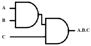
Que.1: Given two X-OR gates, make one as a buffer and one as an inverter.
Answer: If we tie one input of X-OR as 1 then it will act as an Inverter. If we tie one input of X-OR as 0 then it will act as a Buffer.
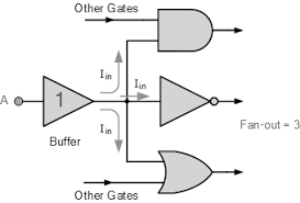
Que.2: Tell some applications of Buffer.
Answer: They are used to introduce delays in digital circuits. They are used to eliminate cross-talk due to inter-electrode capacitance due to close routing. They are used to support high fan-out.
Que.3: Give two methods of converting a two-input NAND gate to an inverter.
Answer: Method 1: Short both the inputs of the NAND gate and apply the signal then it will act as an Inverter. Method 2: Connect the output to one of the inputs and the other to the input signal.
Que.4: Why are most interrupts active low?
Answer: If you consider the transistor level of a module, active low means the capacitor in the output terminal gets charged or discharged based on low-to-high and high-to-low transition respectively. When it goes from high to low it depends on the pull-down resistor that pulls it down and it is relatively easy for the output capacitance to discharge rather than charge. hence people prefer using active low signals.
Que.5: Difference between Latch and Flip-flop.
Answer: The latch is a level-sensitive device whereas the flip-flop is an edge-sensitive device. flip-flops are made up of latches only.
Que.6: What is a multiplexer?
Answer: It is a combinational circuit that selects binary information from one of many input lines and directs it to a single output line.
Que.7: What is a major advantage of R-2R ladder DAC as compared to binary-weighted DAC?
Answer: The R-2R ladder uses only two values of resistors in the circuits while n binary-weighted DAC various values of resistors are required which depends on the number of binary bits.
Que.8: What is the accuracy of a digital-to-analog converter?
Answer: It is the comparison between the actual output of the converter and its expected output.
Que.9: No. of unused states in the 3-bit Jhonson’s counter is?
Answer: To find out the unused states in Jhonson’s Counter we can use the formula: 2n-2n. So unused states in the 3-bit Jhonson’s counter = 23-6 =2
Que.10: What is Digital Gate?
Answer: Digital gates are basically electronic components that are used for switching and manipulating binary data
Que.11: What do you mean by the universal gate?
Answer: The universal gates are those from which we can make any gate by using them. The universal gates are: NAND and NOR
Que.12: What is a magnitude comparator?
Answer: A digital comparator or magnitude comparator is a hardware electronic device that takes two numbers as input in binary form and determines whether one number s greater than, less than, or equal to the other number.
Comparators are used in the central processing units (CPU) and microcontrollers.
Que.13: What is Flip-flop?
Answer: Flip-flop is a sequential device that is used to store 1 bit.
Que.14: How many types of flip-flops are used in digital circuits?
Answer: J-K flip-flop, S-R flip-flop, D flip-flop, T flip-flop.
Que.15: What is the disadvantage of SR flip-flop?
Answer: In SR flip-flop, if both the inputs are at logic 1 then it gives invalid output.
Que.16: What is the disadvantage of the JK flip-flop?
Answer: In JK flip-flop there will be a race around the condition that occurs when both the inputs are at logic 1. To remove race-around conditions, we have to use a master-slave flip-flop or we have to use an edge-sensitive flip-flop.
Que.17: What is the race-around condition of the JK flip-flop?
Answer: For the JK flip-flop, if J=K=1, and if clk=1 for a long period of time, then output Q will toggle as long as CLK remains high which makes the output unstable or uncertain. This is called a race-around condition in the JK flip-flop.
Que.18: What is the Shift register?
Answer: The shift register is a device that is used for storing and processing the bit in serial or parallel.
Que.19: What are the types of Shift registers?
Answer: Serial In Serial Out (SISO), Serial In Parallel Out (SIPO), parallel In Serial Out (PISO), Parallel In Parallel Out (PIPO)
Que.20: What is the Setup Time?
Answer: A minimum time period during which data must be stable before the clock makes a valid transition. For example: For a positive edge-triggered flip-flop having a setup time of 2 ns then input data should be stable for 2 ns before the clock makes a valid transition from zero to one.
Que.21: What is Hold Time?
Answer: A minimum time period during which data must be stable after the clock has made a valid transition. For example: For an edge-triggered flip-flop, with a hold time of 1 ns, then input data should be stable for at least 1 ns after the clock has made the transition.
Que.22 What does Boolean algebra deal with?
Answer: Boolean algebra is the category of algebra in which the variable’s values are the truth values, true and false, ordinarily denoted 1 and 0 respectively. It is used to analyze and simplify digital circuits or digital gates. It is also called Binary Algebra or logical algebra.
Boolean Algebra Operations:
- The basic operations of Boolean algebra are as follows:
- Conjunction or AND operation
- Disjunction or OR operation
- Negation or Not operation
Que.23 What are the different ways of minimizing logical expressions in a digital system?
Answer: To minimize a logical expression 3 different methods are used:
- Boolean algebra: when a number of variables are less and the output is 0 or 1.
- The k-map technique: can be used for up to 5 variables.
- Tabulation method: this method can be used for any number of variables.
Que.24 What are the different Boolean theorems? What is the advantage of using Boolean theorems?
Answer:
- Different Boolean theorems used to minimize the logic expressions are:
- Distribution theorem
- Consensus theorem
- De Morgan’s theorem
- Transposition theorem
- Advantages of using Boolean theorems:
- The number of logic gates was reduced.
- Speed of operation improves.
- Power dissipation decreases.
- Complexity reduces.
Que.25 What is Dual Expression in a digital system? What is a self-dual expression?
Answer:
- Dual expression is used to convert positive logic into negative logic or vice-versa.
- Self-dual expression: when a variable dual is equal to the variable itself, it is called self-dual.
Que.26 What are the inside circuits of logic gates?
Answer:
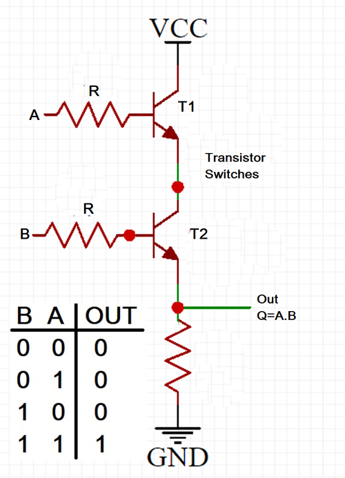
Logic gates are made up of BJT & MOSFET transistor circuits or diode circuits.
For example: AND gate uses BJT.
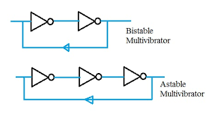
Que.27 How can you design a bistable multivibrator using a NOT gate?
Answer: To design a bistable multivibrator using a NOT gate, even a number of NOT gates are used.
Que.28 Design a square wave generator using NOT gate.
Answer:
- To design a square wave generator or astable multivibrator or free-running oscillator, an odd number of inverters (NOT gates)are used.
- The time period of the inverter is given by:
T= 2\times N \times t_{pd}
Where, N: No. of gates and, t_{pd}: propagation delay of each gate
Que.29 What does universal gate mean? What are the different universal gates in a digital system?
Answer:
- Universal gate: A universal gate is a gate that can implement any Boolean function without the need to use any other type of gate.
- The NAND and NOR gates are universal gates.
- In practice, this is advantageous since NAND and NOR gates are economical and easier to fabricate and are the basic gates used in all IC digital logic families.
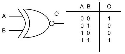
Que.30 Which logic gate is used as a coincidence detector and why it is called a coincidence detector?
Answer:
- XNOR gate is used as a coincidence detector.
- X-NOR Gate is known as the Coincidence Detector. Because It’s true when both inputs is the same.
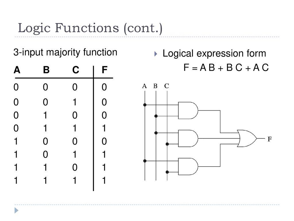
Que.31 What is a 3-bit majority function?
Answer:
- 3-bit majority function: It produces an output if one of the majority of the inputs is one and produces an output of zero if the majority is zero.
Que.32 What is the overflow condition in binary addition?
Answer: Overflow conditions occur in signed arithmetic operations when two same signed numbers are added and the result exceeds a given number of bits.
Que.33 What is the prime & essential prime implicant in K-map?
Answer:
- Prime implicant(PI): it is a product term, which is obtained by combining a maximum number of cells in a K-map.
- Essential prime implicant (EPI): it is a prime implicant that is possible to combine only one way and there is no other alternative.
- It is a compulsory term in minimizing expression.
- For example:

Que.34 What are the hazards of the digital system?
Answer: Hazards are the unwanted switching transients that may appear at the output of the digital circuit. such hazards may result in a malfunction in the output of the circuit.
Also Read: Types of hazards in digital electronics
Que.35 What is a digital comparator circuit? What is the application of comparators in digital electronics?
Answer:
- The digital circuit that performs this comparison task between binary numbers is called a digital comparator.
- Suppose we have two binary numbers which we have to compare according to their magnitude. One number of these two numbers can either be greater, equal, or smaller than the other number. let us consider two single-bit binary numbers A and B. The value of A and B either be 0 or 1 and nothing else.
- Now let us logically design a circuit that will have two inputs one for A and the other for B and have three output terminals, one for A > B condition, one for A = B condition, and one for A < B condition. Let us name the output terminals G, E, and L respectively.
| A | B | G | E | L |
|---|---|---|---|---|
| 0 | 0 | 0 | 1 | 0 |
| 0 | 1 | 0 | 0 | 1 |
| 1 | 0 | 1 | 0 | 0 |
| 1 | 1 | 0 | 1 | 0 |
We want,
G = 1 (logically 1) when A > B.
E = 1 (logically 1) when A = B.
And
L = 1 (logically 1) when A < B.
If we successfully design this logic circuit, it will confidently compare two single-bit binary numbers A, and B, and give a high state at the respective output terminal according to the comparison conditions of A and B.
When, A = 0 and B = 0, then A = B and E = 1
When, A = 0 and B = 1, then A < B and L = 1
When, A = 1 and B = 0, then A > B and G = 1
When, A = 1 and B = 1, then A = B and E = 1
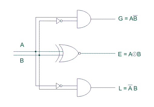
- As the above can only compare two single-bit binary numbers, it is called a single-bit digital comparator.
Que.36 What are the disadvantages of 1’s complement circuit? How can we overcome this problem?
Answer:
The disadvantage of 1’s complement circuit:
- There are 2 0’s representations. (+0 and -0)
- In addition, if carry is present, then it is added to LSB to get the correct result.
- To overcome this problem, 2’s complement representation is used.
Que.37 What is a serial to parallel converter circuit? Why do we do serial to parallel conversion?
Answer:
- The task of a serial-to-parallel converter is to take a stream of data in serial format and for N-bit parallel converter, give N-bits as parallel output. Parallel data is required in several places like communication in a network, radar equipment, etc. But the data cannot be fed to these systems in the parallel format as the external hardware becomes cumbersome. A serial-to-parallel converter comes to the rescue in these situations.
- A serial-to-parallel converter can also be considered as a serial-in parallel-out shift register. The basic structural component of the shift register is a negative edge-triggered D flip-flop. For the N-bit serial to parallel converter, an N number of D flip-flops will be required.
- Serial-in parallel-out can be converted to a serial-in serial-out by only considering the last stage.
NEED FOR SERIAL TO PARALLEL CONVERTER:
- Parallel communication is essential in many systems. Parallel data thus is an inevitable part of many areas. But transmitting data in this format is not feasible in terms of hardware and cost
- productivity. Here comes the need for a serial-to-parallel converter. The transmitter section consists of a vice-versa parallel-to-serial converter and the receiver consists of a serial-to-parallel converter.
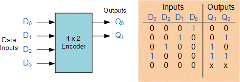
Que.38 What is a priority encoder? What is the application of a priority encoder?
Answer:
- It is an encoder circuit, in which if multiple inputs are logic 1, then the highest priority input line corresponding binary is available at the output.
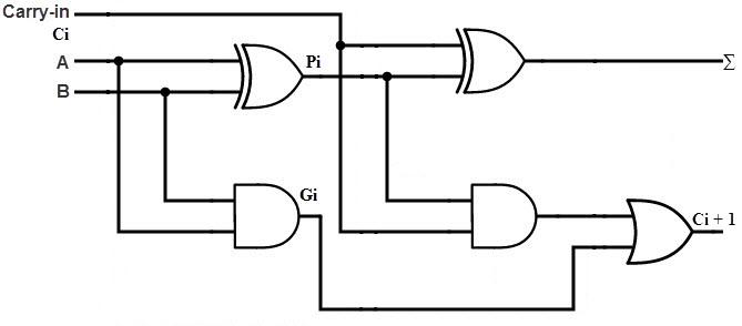
Que.39 Fastest adder in the combinational circuit?
Answer:
- The look-ahead carry adder is the fastest adder because, in this adder, all carry signals are generated in parallel by the look-ahead carry circuit.
- Propagation delay in look-ahead carry adder is independent of a number of bits but depends on the number of levels.
Que.40 What is the difference between combinational circuits and sequential circuits?
Answer:
| Combinational circuit | Sequential circuit |
|---|---|
| Present output depends on present input. | Present output depends on previous input as well as present input. |
| No feedback is present. | Feedback is present. |
| It has no memory. | It has a memory. |
| No clock control is needed in combinational circuits. | Clock control is used to synchronize the input signal. |
| Example: multiplexer, decoder | Examples: flip-flops, counters |
Que.41 Which logic gate only follows commutative law but not associative law?
Answer: The NAND gate is the only logic gate that follows commutative law but is not associative law.
Que.42 What is a latch?
Answer:
- The latch is a 1-bit memory element.
- It is the cross-coupled connection of logic gates that are used to store bit 1 or zero at a time.
Types of latch:
- Active high-standard latch
- Active low standard latch.
Que.43 Which logic family is the fastest one and why?
Answer: The emitter-coupled logic (ECL) family is the fastest one because it has a propagation delay of 100 pico sec, which is much less compared to all other logic gates.
Que.44 Which logic family has the best figure of merit and why?
Answer:
- The figure of merit is nothing but the product of propagation delay and power dissipation.
- Integrated injection logic has high FOM i.e. of 0.1 to 0.7 PJ. The reason is, that this logic family uses the current source to make the transistor on, hence low power dissipation.
Que.45 Which logic family has the lowest power dissipation and why?
Answer:
- CMOS has the lowest power dissipation.
CMOS has low power dissipation because:
- In C, you have High Z input and active pull-up and Pulldown so you don’t have any static power usage and the only power usage is dynamic power usage( charging and discharging load capacitor).
- CMOS is full-swing technology ( in the output you have exact VDD and GND).
- Do not use any resistor in CMOS so the size of your circuit becomes very small.
Que.46 What is fanout in logic families?
Answer:
- Fanout: It is the number of logic gates that can be connected to a logic gate output without affecting its operation.
- Fanout of any logic gate depends on the current source and sink capability of the logic gate.
Que.47 What is the noise margin in logic families?
Answer:
- It is the maximum noise voltage that can be added to the logic gate input which will not affect the output.
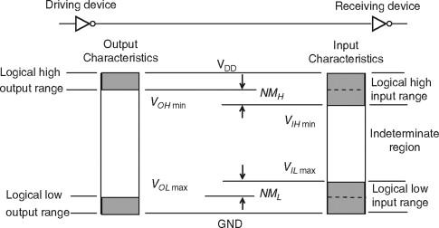
NMH= VOH– VIH
NML= VIL– VOL
- And overall noise margin is given by the minimum of these two.
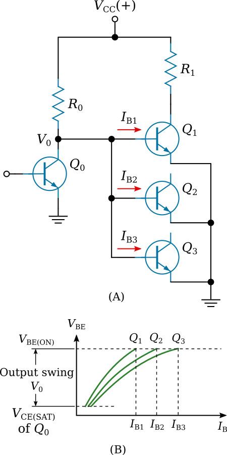
Que.48 What is the current hogging problem? In which logical family does it occur? How it can be avoided?
Answer:
- Current hogging occurs in the direct transistor logic (DCL) family.
- This phenomenon arises because of the spread in VBE(ON) of the various driven (fan-out) transistors. No two transistors will ever have identical input characteristics, and it is always desirable to use transistors with as small a production spread as possible on VBE(ON).
- If the transistors Q1, Q2, and Q3 in the figure below (view A) have input characteristics as shown in the figure below (view B), it is quite clear that the output voltage swing V0 of transistor Q0 will be determined by the VCE(SAT) of Q0 and the VBE(ON) of one of the fan-out transistors. The figure below (view B) shows that the voltage V0 will be determined by the VBE(ON) of Q3, which will draw more current from R0 than from either Q2 or Q1. It is quite possible that the unequal currents demanded by the fan-out transistors may result in some units hogging more current and thereby starving the other transistors, which may not get the sufficient base drive to saturate them, or in some cases, even turn them on at all.
Que.49 What is a register in digital electronics? What are the different types of registers?
Answer: Registers are cascading flip-flops used to store groups of bits. To store n-bit in registers maximum n flip-flops are used.
- Registers are classified as:
- SISO( serial in serial out)
- SIPO(serial in parallel out)
- PISO(parallel in serial out)
- PIPO( parallel in parallel out)
Que.50 What are the essential features of a memory element?
Answer: Essential features of memory elements are:
- It should store the data once the excitation is applied.
- It should retain data even if excitation is removed.
- To store the new data, new excitation should be applied.
Que.51 What is a counter circuit? What is its application?
Answer: The counter circuit is a cascading of flip-flops that have the following functions:
- It is used to count the number of clock pulses applied.
- It is used for waveform generation.
- It is used in timer and control circuits.
Applications of counter:
- It is used in analog to digital converters.
- It is used for frequency and range measurement in RADAR.
- It is used for pulse width measurement.
- It is also used as a frequency divider.
Que.52 What is the difference between synchronous counter & asynchronous counter?
Answer:
| ASYNCHRONOUS COUNTER | SYNCHRONOUS COUNTER |
|---|---|
| Different flip-flops have different clocks. | All flip flops are applied with the same clock. |
| It is slower than synchronous. | It is faster than an asynchronous counter. |
| The transition state is present due to propagation delay. | It has no transition state. |
| Any fixed count sequence is possible. | Any count sequence is possible. |
| Clock time period = n x propagation delay | Clock time period = propagation delay |
Que.53 What is a Ring counter? Applications of the Ring counter.
Answer:
- In a Ring counter, only one flip-flop is logic 1 and it will rotate among all flip-flops when the clock is applied.
- It is the fastest counter.
Applications of Ring Counter:
- It is used in stepper motor control.
- Used in waveform generator.
- Used in successive approximation type ADC.
Que.54 Difference between synchronous clock and asynchronous clock.
Answer:
- If the two clocks have the same phase and frequency may or may not be the same, then the clock is called a synchronous clock. i.e. if the source of the two clocks is the same, then it is synchronous.
- If the two clocks have different phases, the frequency may or may not be the same. it is called an asynchronous clock.
Que.55 What is a glitch?
Answer:
- A glitch is an unpredictable output.
- Some input for which we predict a known output, but before output settles to what we expect, it goes through one or more transitions. These are called glitches.
- Because the inputs have to go through different gates and the propagation delay of each can be different, therefore results arrive at the final gate at different times.
- If glitches are not removed, they will go to the next circuit stage and generate more unpredictable results.

Que.56 What are finite state machines? Types of FSM.
Answer:
- A state machine is a behavioral model. It consists of a finite number of states hence called an FSM( finite state machine).
- Based on the current states and inputs, the machine performs state transitions and produces outputs.
- Basically, there are two types of FSM:
- Mealy state machine: this present output depends upon the present state and next input.
- Moore state machine: in this type of state machine, the present output depends only on the present state.
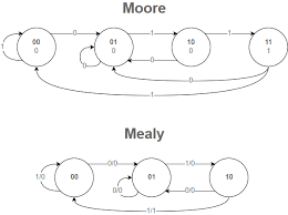
- In the given circuit, we can see that Mealy has input as well as a present state while Moore has a present state only.
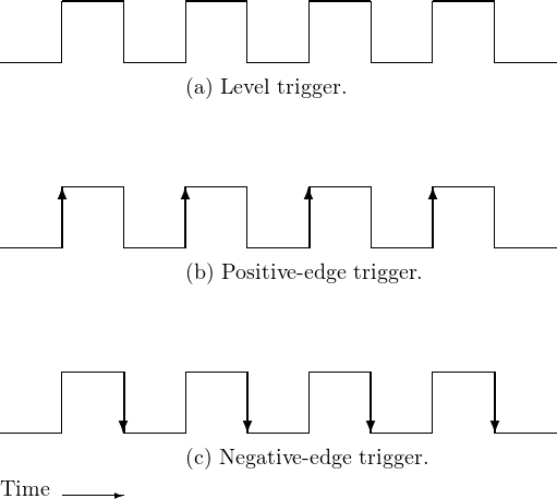
Que.57 What is the difference between level-triggered and edge-triggered circuits?
Answer:
- Level Triggering: In level triggering the circuit will become active when the gating or clock pulse is on a particular level. This level is decided by the designer. We can have a negative level triggering in which the circuit is active when the clock signal is low or a positive level triggering in which the circuit is active when the clock signal is high.
- Edge Triggering: In edge triggering the circuit becomes active at the negative or positive edge of the clock signal. For example, if the circuit is positive edge triggered, it will take input at exactly the time at which the clock signal goes from low to high. Similarly, input is taken at exactly the time at which the clock signal goes from high to low in negative edge triggering. But keep in mind after the input, it can be processed all the time till the next input is taken.
Que.58 Types are memories in a digital circuit.
Answer: Different types of memories used in the digital circuits are:
- Registers: fastest memory
- Primary memory: can be further classified as:
- RAM- random access memory
- ROM- read-only memory
- Secondary memories: this is the slowest one. Example: magnetic tapes.
Que.59 Difference between RAM and ROM.
Answer:
| RAM | ROM |
|---|---|
| perform both functions read and write. | Performs only read operation. |
| The temporary storage of files. | Permanent storage of files. |
| It is a volatile memory. | It is a non-volatile memory. |
| Responsible for user data storage. | It stores system programs. |
| Random access. | It also has random access. |
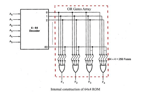
Que.60 ROM is made up of a combinational circuit how it is a memory?
Answer: ROM (read-only memory) is a universal circuit, not memory but behaves like a memory. It has combinational circuit components a suitable size decoder and OR gate. It is called memory because the input encodes a memory address and the output encodes the value stored at that address.
Que.61 What is the difference between static RAM and dynamic RAM?
Answer:
| STATIC RAM | DYNAMIC RAM |
|---|---|
| Data is stored in cross-coupled logic ckt. | Data is stored in capacitors. |
| It is made up of BJT & MOSFET. | It is made up of MOSFETs only. |
| 6 transistors are used to store on a bit. | Require only 2 transistors. |
| Faster than DRAM | Slower than SRAM. |
| Memory capacity is less. | Memory capacity is more. |
| Dissipates more power. | It dissipates less power. |
| Refreshing is not required. | It requires refreshing. |
| It is a volatile memory | It is a volatile memory. |
| used as cache memory. | It is part of the main memory. |
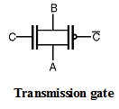
Que.62 What is a transmission gate in the digital circuit?
Answer: The transmission gate is mainly a bi-directional switch enabled by the gate signal ‘C’. When C = 1 both MOSFETs are ON and the signal passes through the gate i.e. A = B if C = 1. Whereas C = 0 makes the MOSFETs cut off creating an open circuit between nodes A and B.
Que.63 What is a pass transistor logic circuit? Advantages of using pass transistor logic.
Answer:
- The Pass transistor logic is required to reduce the transistors for implementing logic by using the primary inputs to drive gate terminals, and source and drain terminals. In complementary CMOS logic, primary inputs are allowed to drive only gate terminals.
- The figure below shows an implementation of the AND function using only NMOS pass transistors. In this gate, if the B input is high the left NMOS is turned ON and copies the input A to the output F. When B is low the right NMOS pass transistor is turned ON and passes a ‘0’ to the output F.

- The major advantage of pass transistor logic is that fewer transistors are required to implement a given function.
Que.64 What are the advantages and disadvantages of the K-map method of Boolean simplifications
Answer:
- The advantages of K-map are shown below:
- K-map simplification does not demand the knowledge of Boolean algebraic theorems.
- Usually, it requires less number of steps when compared to the algebraic minimization technique.
- Disadvantages of Karnaugh Map:
- The complexity of the K-map simplification process increases with the increase in the number of variables
- The minimum expression obtained might not be unique
Que.65 What are the characteristics of digital ICs?
Answer:
- Characteristics of digital ICs:
For more details on the Characteristics of Digital ICs, you can click the below link to know more about it.
Also Read: Characteristics of digital IC
Que.66 Which code is called a minimum change code and why?
Answer: A grey code is called a minimum change code. It is called so because only one-bit changes during any transition between two numbers.
Que.67 What is an inhibitor circuit?
Answer:
- Many times there arise many situations when the logical signals need to be either enabled or inhibited which depends upon certain other control inputs. This is where the need for this type of logic gate arises.
- Inhibitor circuit- It is basically an AND gate that has one of its inputs negated by an inverter. The input which is negated acts to inhibit the gate. Or we can say the gate will behave like an AND gate only when the negated input is set at a logic level ‘0’.
Que.68 What is the advantage of fixed-point representation over floating-point representation?
Answer:
- The fixed point is a representation of a floating-point number in integer format. So operations can be applied to the number just like on integers. The advantage of using this is that floating-point arithmetic is costlier (processing power). Newer processors have dedicated FPUs (floating-point units) for handling that. So fixed-point arithmetic is when processing power is limited, and a little precision loss doesn’t cause havoc.
- Fixed pointed numbers can be sorted in linear time. The fixed point is also unambiguous; each numerical value that can be expressed in a specific fixed point protocol has only one representation, which isn’t true with floating point.
- Floating-point has a much wider representable range. It is also ambiguous. Floating-point numbers can be sorted in NlogN time.
- Floating-point numbers are good for, well, floating points, i.e. when you need to express numbers across varying scales. You sacrifice precision to gain a range of scale.
- On the other hand, fixed-point numbers are only suitable at a fixed scale (and they’ll over or underrun if you scale them too much), but you gain precision as long as you remain within the desired scale.
- In short: If you multiply a lot but don’t add numbers of different scales, use floating points. If you add a lot but don’t multiply, use fixed points.
Que.69 What do you mean by clock skew and clock jitter?
Answer:
- Clock skew: Clock skew is where the timing of a clock is out of phase with the system reference. It can originate from different sources and limits the clock frequency. In a synchronous system, this is equivalent to limiting the data flow rate and the overall speed.
- Clock jitter: Clock jitter refers to the temporal variation of the clock period at a given point i.e. the clock period can expand on a cycle-by-cycle basis. It is strictly a temporal uncertainty measure and is often specified at a given point on the chip. Jitter directly impacts the performance of a sequential system.
Que.70 What is Schottky TTL?
Answer:
- Schottky TTL: it is a relatively fast bipolar logic family, normally produced in integrated-circuit form, whose internal configuration is similar to normal TTL except that Schottky transistors are used.
Que.71 What is the range of temperature over which logic families work satisfactorily?
Answer: The temperature range over which logic families is 0-70 degrees Celcius.
Que.72 What are degenerate forms in two-level logic implementation?
Answer:
- For two-level logic implementation, we consider four logic gates i.e., AND Gate, OR Gate, NAND Gate, and NOR Gate. If we use one of these four gates at the first level and one at the second level then we get a total of 16 combinations of two-level logic.
- Degenerate form: The two-level combination that degenerates into a single logic function is known as degenerate form.
- There are 8 degenerate forms in those 16 combinations.
- For example AND-AND
- Here are two-level AND-AND ckt. can be converted to a single logic function.
Que.73 What are the requirements of a logic family?
Answer: The requirements of a logic family are:
- Supply voltage range.
- Speed of response.
- Dissipation of power.
- Input and output logic levels.
- Current sinking capability.
- Current sourcing capability.
- Flexibility.
- Noise immunity.
Que.74 What is a sequence generator circuit? Application of sequence generator?
Answer:
- The sequence generator is a circuit that generates a desired sequence of bits at its output in synchronization with the clock.

- Some of the applications of the sequence generator are as follows :
- Random bit generator
- Counters
- Code generators
- Period and sequence generator.
Que.75 Sequence detector circuit and its type.
Answer: A sequence detector accepts as input a string of bits: either 0 or 1. Its output goes to 1 when a target sequence has been detected.
- There are two basic types:
- Overlapping type
- Non-overlapping type
Que.76 What is a PLA circuit? What is the function of the PLA circuit?
Answer: A programmable logic array is a kind of programmable logic device used for the implementation of combinational circuits using buffer, AND, and OR gates.
- It has a programmable AND and fixed OR circuit.
- Applications of PLA Circuit:
- PLA is used to provide control over the datapath.
- PLA is used as a counter.
- PLA is used as a decoder.
- PLA is used as a BUS interface in programmed I/O.
Que.77 What are the disadvantages of ripple carry adder?
Answer: The disadvantage of ripple carry adder:
In a ripple carry adder, as the number of bits is increased, the rate of addition will decrease or the delay will increase.
Que.78 What are the functions of a parity generator and parity checker circuit?
Answer:
- The parity generator and parity checker’s main function is to detect errors in data transmission.
- The parity generator is a combination circuit at the transmitter, it takes an original message as input and generates the parity bit for that message and the transmitter in this generator transmits messages along with its parity bit.
- The combinational circuit at the receiver is the parity checker. This checker takes the received message including the parity bit as input. It gives output ‘1’ if there is some error found and gives output ‘0’ if no error is found in the message including the parity bit.
Que.79 Types of the number system used in digital circuits.
Answer: There are mainly 4 types of number systems:
- Binary system
- Octal number system
- Decimal number system.
- Hexadecimal number system.
Que.80 Why do we use the octal number system in digital electronics?
Answer: Octal numbers are easier to use than decimal and hexadecimal numbers because they use fewer digits. In other words, it makes fewer computations and makes fewer errors. The program only uses three bits to represent any digit in binary, and it can be converted from octal to binary and vice versa in seconds.
Que.81 Which number system is used by digital computers to encode data and programs?
Answer: A binary number system is used to encode data and programs. Binary numbering systems are best suited to the digital signal coding of binary, as they use only two digits, one and zero, to form different figures.
Que.82 What Is The Purpose Of Hexadecimal Number System?
Answer: Computer system designers and programmers use hexadecimal numerals because they provide a human-friendly representation of binary values. Each hexadecimal digit represents four bits (binary digits), also known as a nibble (or nybble).
Que.83 What is the disadvantage of the octal number system?
Answer: The major disadvantage of the Octal number system is that the computer does not understand the octal number system directly, so we need an octal-to-binary converter.
Que.84 How a decoder is used in memory management?
Answer: A Decoder is used in memory management to reach a particular memory address, row and column decoders are used to select a particular memory location in an array.
Que.85 How is data written in ROM?
Answer:
- It contains two basic components: the decoder and the OR logic gates.
- In ROM, the decoder receives input in binary form; the output will be the decimal equivalent. The OR gates in ROM use the decoder’s decimal output as their input.ROM performs like a disk array. It contains a grid of rows and columns that are used to turn the system on and off.
- Every element of the array correlates with a specific memory element on the ROM chip. A diode is used to connect the corresponding elements. When a request is received, the address input is used to find the specific memory location.
- The value that is read from the ROM chip should match the contents of the chosen array element.
Que.86 Are decoder and demultiplexer are same?
Answer:
- Decoder: The decoder is a combinational logic circuit and its purpose is to decode the data given to it. It is made of n number of input lines and 2*n number of output lines. For every probable input condition, there are various output signals, and depending on the input only one output signal will produce the logic. So, this n-to-2n decoder is also called a min-term generator where each output outcomes only at a particular input.
- Demultiplexer: This Demultiplexer is kind of the same as the decoder, but it contains select lines as well. It is used to send a single input over the multiple output lines. It accepts data from one input signal and transfers it over the provided number of output lines. It contains data input lines, select lines, and output lines.
Que.87 Design a 2*1 MUX using a transmission gate.
Answer:

- Here, in this case, C is used as a control signal and A & B are inputs. We will get one output at a time.
Que.88 Can a transmission gate act as a universal gate?
Answer: Yes, a transmission gate can act as a universal gate because all other logic gates such as AND, OR, NOT, NOR, etc. can be derived using a transmission gate.
Que.89 What is the use of a transmission gate?
Answer:
Application of transmission gate:
- Transmission gates are typically used as building blocks for logic circuitry, such as a D Latch or D Flip-Flop. As a stand-alone circuit.
- A transmission gate can isolate a component or components from live signals during hot insertion or removal.
- In a security application, they can selectively block critical signals or data from being transmitted without proper hardware-controlled authorization.
Que.90 What is VLSI technology? What is the reason behind its popularity?
Answer:
- VLSI: Very-large-scale integration technology is a process of creating integrated circuits by using thousands of transistors on a single chip.
- It uses a minimum of 1000 gates for integration.
- The electronics industry has achieved phenomenal growth over the last few decades, mainly due to the rapid advances in large-scale integration technologies and system design applications. With the advent of very-large-scale integration (VLSI) designs, the number of applications of integrated circuits (ICs) in high-performance computing, controls, telecommunications, image and video processing, and consumer electronics has been rising at a very fast pace.
Que.91 Application of CMOS inverter.
Answer:
- CMOS inverters play a critical role in integrated circuits, including microprocessors, microcontrollers, static RAM, image sensors, data converters, and some types of transceivers.
- CMOS inverters are found in digital cameras, mobile devices, home computers, network servers, routers, modems, cell phones, and virtually every other electronic device that requires logic functions.
Que.92 What is the size of ROM for the n-bit full adder?
Answer:
- To find the size of the ROM we need to find the number of inputs and output bits –
- Number of inputs = n(A) + n(B) + 1(Cin) = 2n+1 address bits
- Number of outputs = n(sum/diff) + 1(Cout) = n+1
- Thus, this would require a 2^(2n+1) x (n+1) -bit ROM.
Here, n(A) means the number of inputs for A, and n(B) means the number of inputs for B.
- Example: The size of the ROM you could use to program for an 8-bit adder/subtractor with Cin and Cout is given by
Number of inputs = 8 (A) + 8 (B) + 1(Cin) = 2(8)+1 = 17 address bits.
Number of outputs = 8 (sum/diff) + 1(Cout) = 8+1 = 9
Thus, this would require a 2^(2n+1)x(n+1) = 2^(17)x9 bit ROM.
Que.93 Which decoder should we use to design a full adder?
Answer:
- A full adder adds three one-bit binary numbers, two operands, and a carry bit. The adder outputs two numbers, a sum and a carry bit.
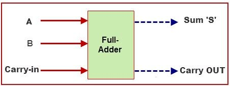
- A decoder circuit takes binary data of ‘n’ inputs into ‘2n’ unique output.
- Hence to design a full adder using a decoder We use a 3:8 decoder. Where inputs are A, B, and carry in and output is the sum and carry.

Que.94 What is EPROM? What is its application?
Answer:
- EPROM stands for Erasable read-only memory which is a nonvolatile memory chip. In this type of ROM, ultraviolet rays are used to erase the data, so that data can be reprogrammed.
- It uses a MOS transistor to reprogram the data.
- EPROM can be erased and reprogrammed multiple times without a problem.
Applications of EPROM:
- EPROM is used in computer BIOS in order to store a bootloader which will initialize the computer and load a very basic BIOS operation system to load the normal operating system.
- Microcontrollers use EPROMs in order to store some data which can be stored over reboots.
- EPROM has also been used in games especially low-level graphical games in order to store game data, code, and programs.
- EPROM is mainly used in personal and enterprise computers to assist other devices.
Que.95 difference between EPROM and EEPROM.
Answer:
| EPROM | EEPROM |
|---|---|
| Data is erased using UV rays. | Data is erased by using electrical signals. |
| Erasing time is 15-20 minutes. | Erase data in seconds only. |
| first total memory is erased then reprogramming is performed. | No need to erase total memory, erasing can be performed at any particular instant. |
Que.96 What are the characteristics of ADC?
Answer: Characteristics of ADC:
Resolution: The resolution of a converter represents the number of different values it can produce over a large number of analog inputs.
Conversion time: it depends upon the type of ADC used and method of conversion, the material on the chips.
Reference voltage: The larger the reference voltage we give as input, we get the larger the value of step size.
Digital output data: output data depends on the number of bits. For an 8-bit ADC, output data is from D0-D7.
Que.97 What are the applications of DAC in real life?
Answer: DACs play an important role in many digital signal processing applications.
- Audio Amplifier: DACs are used to produce DC voltage gain with Microcontroller commands. Often, the DAC will be incorporated into an entire audio codec which includes signal processing features.
- Video Encoder: The video encoder system will process a video signal and send digital signals to a variety of DACs to produce analog video signals of various formats, along with optimizing output levels. As with audio codecs, these ICs may have integrated DACs.
- Display Electronics: The graphic controller will typically use a lookup table to generate data signals sent to a video DAC for analog outputs such as Red, Green, and Blue (RGB) signals to drive a display.
Data Acquisition Systems-Data to be measured is digitized by an Analog-to-Digital Converter (ADC) and then sent to a processor. The data acquisition will also include a process control end, in which the processor sends feedback data to a DAC for converting to analog signals.
- Calibration: The DAC provides dynamic calibration for gain and voltage offset for accuracy in test and measurement systems.
- Digital potentiometer: works on the principle of DAC.
- Motor control: many motor controls require voltage control which is provided by DAC.
Que.98 What are the factors affecting the accuracy of ADC?
Answer: Factors affecting the accuracy of an ADC are:
- Resolution
- Quantization
- Offset and gain error
- Non-linearity
- System noise
Que.99 What are the ADC specifications?
Answer: ADC specifications are as follows:
- Resolution
- Conversion time and conversion latency
- Aperture jitter
- Aperture delay
- Power supply rejection
- Common mode rejection
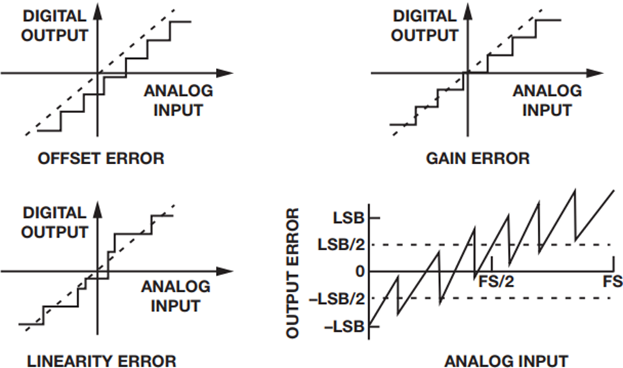
Que.100 What are the errors in ADC?
Answer: Errors in ADC are:
- Quantization error: Quantization error is the difference between the analog signal and the closest available digital value at each sampling instant from the A/D converter.
- Offset error: Analog-to-digital converter (ADC) offset error is defined as the deviation of the actual ADC’s transfer function from the perfect ADC’s transfer function at the point of zero to the transition measured in the Least Significant Bit (LSB). When the transition from output value 0 to 1 does not occur at an input value of 0.5 LSB, then we say that there is an offset error.
- Gain Error: Gain error is the difference in the slope of the actual transfer function and the ideal transfer function.+
- Differential nonlinearity: The DNL is the maximum deviation of the output steps from the ideal analog LSB value.
- Integral non-linearity: The INL is defined as the maximum deviation of the actual input-output characteristic from the ideal transfer characteristic.
Que.101 What is quantization error in ADC and how does it relate to signal-to-noise ratio?
Answer:
- Quantization error is the difference between the analog signal and the closest available digital value at each sampling instant from the A/D converter.
- Quantization error also introduces noise, called quantization noise, to the sampled signal. The higher the resolution of the A/D converter, the lower the quantization error and the smaller the quantization noise.
- The relationship between resolution (in bits) and quantization noise for an ideal A/D converter can be expressed as –
Signal to Noise (S/N) = -20*log (1/2^n)
where n is the resolution of the A/D converter in bits.
- S/N is the signal to noise and is expressed in dB.
- This relationship can also be approximated as S/N = 6*n.
- Typical S/N ratios for ideal A/D converters are 96dB for 16 bits, 72dB for 12 bits, and 48dB for 8 bits.